


 It’s Only Common Sense: OCCAM—the Time Is Now
 Marcy's Musings: The Growing Industry
 Dan’s Biz Bookshelf: Seeing the How
Biodegradable Electronics
October 13, 2017 | Fraunhofer FEPEstimated reading time: 1 minute
Under the direction of the Fraunhofer Institute for Organic Electronics, Electron Beam and Plasma Technology FEP, an in-house Fraunhofer project for development of biodegradable electronics was begun last year. The Fraunhofer Institute for Electronic Nano Systems ENAS, the Fraunhofer Institute for Biomedical Engineering IBMT, the Fraunhofer Institute for Silicate Research ISC, and the Fraunhofer Resource Recycling and Strategy Project Group IWKS are working together on the project.
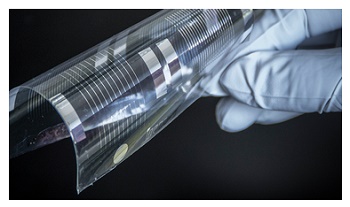
Electronic components that are completely broken down in a biological environment after a pre-defined operating life open up novel applications as well as ways for reducing their ecological footprint.
One enabling technology for such components is the manufacture of biodegradable conductive traces on biodegradable substrates using vacuum technologies. This technology was developed by Fraunhofer FEP.
A novel application area for these innovative electronic components for example is in the field of active medical implants that after expiration of their operating life are resorbed by tissue, thereby sparing the patient a second surgical intervention.
The Fraunhofer Gesellschaft e. V. is now funding the "bioElektron - Biodegradable Electronics for Active Implants" project through its in-house program (funding No. MAVO B31 301). The goal of the project is the development of essential components for biodegradable electronic parts that can be employed for example in an implant.
This includes in particular:
- biodegradable conductor structures
- biodegradable electrodes for collecting electrical signals or delivering electrical stimulation
- biodegradable thin-film transistors and circuitry
- biodegradable barrier coatings as moisture and gas barriers, and electrical insulation layers
These elements will be monolithically integrated into a flexible thin-film device.
Conductor structures and organic thin-film transistors are being developed at Fraunhofer FEP using vacuum technology. Deposition of magnesium via thermal evaporation under high vacuum conditions is being used as an enabling technology for this purpose. Magnesium is known for being a biodegradable and biologically compatible metal that is already employed in clinical environments as an absorbable implant material. The challenge consists of depositing this metal upon biodegradable polymer films that magnesium does not adhere sufficiently to under normal process control. By suitably pre-treating the substrates using a combination of drying, plasma treatment, and utilization of seed layers, finely structured high-quality conductor structures were able to be produced.
Share on:


Suggested Items
Koh Young Showcases Award-winning Inspection Solutions at SMTconnect with SmartRep in Hall 4A.225
04/25/2024 | Koh Young TechnologyKoh Young Technology, the industry leader in True 3D measurement-based inspection solutions, will showcase an array of award-winning inspection and measurement solutions at SMTconnect alongside its sales partner, SmartRep, in booth 4A.225 at NürnbergMesse from June 11-13, 2023. The following offers a glimpse into what Koh Young will present at the tradeshow:
Real Time with… IPC APEX EXPO 2024: Plasmatreat: Innovative Surface Preparation Solutions
04/25/2024 | Real Time with...IPC APEX EXPOIn this interview, Editor Nolan Johnson speaks with Hardev Grewal, CEO and president of Plasmatreat, a developer of atmospheric plasma solutions. Plasmatreat uses clean compressed air and electricity to create plasma, offering environmentally friendly methods for surface preparation. Their technology measures plasma density for process optimization and can remove organic micro-contamination. Nolan and Hardev also discuss REDOX-Tool, a new technology for removing metal oxides.
Nanotechnology Market to Surpass $53.51 Billion by 2031
04/25/2024 | PRNewswireSkyQuest projects that the nanotechnology market will attain a value of USD 53.51 billion by 2031, with a CAGR of 36.4% over the forecast period (2024-2031).
Cadence, TSMC Collaborate on Wide-Ranging Innovations to Transform System and Semiconductor Design
04/25/2024 | Cadence Design SystemsCadence Design Systems, Inc. and TSMC have extended their longstanding collaboration by announcing a broad range of innovative technology advancements to accelerate design, including developments ranging from 3D-IC and advanced process nodes to design IP and photonics.
SMC Korea 2024 to Highlight Semiconductor Materials Trends and Innovations on Industry’s Path to $1 Trillion
04/24/2024 | SEMIWith Korea a major consumer of semiconductor materials and advanced materials a key driver of innovation on the industry’s path to $1 trillion, industry leaders and experts will gather at SMC (Strategic Materials Conference) Korea 2024 on May 29 at the Suwon Convention Center in Gyeonggi-do, South Korea to provide insights into the latest materials developments and trends. Registration is open.