


 It’s Only Common Sense: OCCAM—the Time Is Now
 Marcy's Musings: The Growing Industry
 Dan’s Biz Bookshelf: Seeing the How
Visible Graphene Plasmons from Electrons
October 16, 2017 | ICFOEstimated reading time: 1 minute
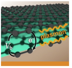
ICFO researchers propose a method to generate graphene visible plasmons from electron tunnelling.
The research of light-matter interactions with nanostructures has become essential in the field of photonics. In such interactions, plasmons play a major role because they are capable of concentrating optical fields down to nanometer-sized regions and enhancing the intensity of incident light by several orders of magnitude.
High-quality graphene plasmons offer the advantages of being electrically, magnetically, and optically tunable, but these outstanding properties are only sensitive to the mid-infrared range. Such properties become very week when trying to use light interactions to generate graphene plasmons in the visible regime.
In a recent study published in ACS Photonics, selected as Editor’s choice by this journal and highlighted in Nature Nanotechnology Research Highlights, ICFO researchers Sandra de Vega and ICREA Prof. at ICFO F. Javier García de Abajo from the Nanophotonics Theory research group at ICFO, have proposed a new theoretical methodology to generate visible plasmons in graphene not from light but from tunnelling electrons.
Through theoretical simulations, the team of researchers was able to show that graphene plasmons can be efficiently excited via electron tunnelling in a sandwich structure formed by two graphene monolayers separated by a few atomic layers of hexagonal boron nitride (hBN). In their study, they have found a voltage window in which the tunnelling electrons lose energy through the excitation of a propagating optical plasmon rather than dissipate through coupling with the hBN phonons (low bias) or electron–electron interactions (high bias).
Devices that generate plasmons without the use of light can also be used as sensors, where a change in the graphene plasmon properties is translated into a voltage readout. The short wavelength of graphene plasmons relative to the light wavelength makes them attractive for applications in optoelectronics and sensing.
Share on:


Suggested Items
Boeing Opens Research & Technology Center in Japan
04/23/2024 | BoeingBoeing today opened a Boeing Research & Technology (BR&T) Center in Japan that will focus on innovation to enable the commercial aviation industry meet its goal of net zero carbon emissions by 2050.
Gartner Forecasts Worldwide IT Spending to Grow 8% in 2024
04/17/2024 | Gartner, Inc.Worldwide IT spending is expected to total $5.06 trillion in 2024, an increase of 8% from 2023, according to the latest forecast by Gartner, Inc. This is an increase from the previous quarter’s forecast of 6.8% growth and puts worldwide IT spending on track to surpass $8 trillion well before the end of the decade.
Argonne, RIKEN Sign a Memorandum of Understanding in Support of AI for Science
04/16/2024 | BUSINESS WIRELeaders in high performance computing in the U.S. and Japan have signed a memorandum of understanding (MOU) establishing a cooperative relationship in support of artificial intelligence (AI) computing projects.
RAICo Fellowship to Widen Participation Within the Field of Robotics and Artificial Intelligence
04/12/2024 | RAICoWOMEN and those early in their academia career who are passionate about robotics and artificial intelligence are encouraged to apply for a RAICo Fellowship.
Indium to Host Free Webinar on Lead-Free Solder Paste for Automotive Applications
04/09/2024 | Indium CorporationIndium Corporation’s Senior Research Metallurgist, Jie Geng, Ph.D., will conduct a webinar on low-voiding, high-reliability, lead-free solder paste for automotive applications.