


 Marcy's Musings: The Growing Industry
 It’s Only Common Sense: Here’s What To Do After IPC APEX EXPO 2024
 Dan’s Biz Bookshelf: Seeing the How
3D Microprinting: Security for Products, Passports, and Money
November 16, 2017 | KITEstimated reading time: 2 minutes
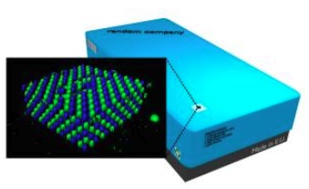
Security features are to protect bank notes, documents, and branded products against counterfeiting. Losses caused by product forgery and counterfeiting may be enormous. According to the German Engineering Association, the damage caused in 2016 in its branch alone amounted to EUR 7.3 billion. In the Advanced Materials Technologies journal, researchers of Karlsruhe Institute of Technology (KIT) and the ZEISS company now propose to use printed 3D microstructures instead of 2D structures, such as holograms, to improve counterfeit protection.
“Today, optical security features, such as holograms, are frequently based on two-dimensional microstructures,” says Professor Martin Wegener, expert for 3D printing of microstructures at the Institute of Nanotechnology of KIT. “By using 3D-printed fluorescent microstructures, counterfeit protection can be increased.” The new security features have a side length of about 100 µm and are barely visible with the eye or a conventional microscope. For their production and application, Wegener and his team have developed an innovative method that covers all processes from microstructure fabrication to the readout of information.
The microstructures consist of a 3D cross-grid scaffold and dots that fluoresce in different colors and can be arranged variably in three dimensions within this grid. To produce and print such microstructures, the experts use a rapid and precise laser lithography device developed and commercialized by the Nanoscribe company, a spinoff of KIT. It enables highly precise manufacture of voluminous structures of a few millimeters edge length or of microstructured surfaces of several cm² in dimension.
The special 3D printer produces the structures layer by layer from non-fluorescent and two fluorescent photoresists. A laser beam very precisely passes certain points of the liquid photoresist. The material is exposed and hardened at the focus point of the laser beam. The resulting filigree structure is then embedded in a transparent polymer in order to protect it against damage.
“Security features produced in this way are not only of individual character, but also very complex in manufacture. This makes life difficult to forgers,” says Frederik Mayer of the Institute of Nanotechnology of KIT. The new process can be extended easily and is extremely versatile. The 3D features may be applied as an embedded foil in security tags to protect pharmaceuticals, car spare parts, or mobile accumulators against counterfeiting. They may also be integrated into the transparent windows of bank notes. For later authentication checks at the supermarket checkout or in the production hall, special readout instruments are required to detect the fluorescent 3D structures.
Share on:


Suggested Items
Mycronic Receives Order for an SLX Mask Writer
04/11/2024 | MycronicMycronic AB has received an order for an SLX mask writer from a new customer in Asia. The order value is in the range of USD 7-9 million. Delivery of the system is planned for the second quarter of 2025.
Plastronics and the New IPC Guidelines for In-mold Electronics (IME)
04/11/2024 | Barry Matties, I-Connect007In the ever-evolving world of electronics, the roads for the integration of electronics assemblies into 3D structures continue to grow into a set of technologies used to produce 3D plastronics parts and revolutionize mainly the automotive industry. IPC has been developing standards for this set of technologies, led by Francisco Fourcade, IPC electronics technology standards manager.
MKS Introduces ESI Geode G2 CO2 Laser System for High- Precision and High-Speed HDI and mSap Via Drilling
04/09/2024 | MKS Instruments, Inc.MKS Instruments, Inc., a global provider of technologies that transform our world, today announced the official launch of the ESI Geode™ G2 laser drill system, the next generation of the Geode™ platform for processing PCB and ICP materials.
MKS’ Atotech, ESI to Participate in IPC APEX EXPO
03/29/2024 | MKS’ AtotechMKS’ Atotech and ESI will participate in this year’s IPC APEX EXPO 2024, the PCB industry’s largest event in North America, to be held in Anaheim, California, to be held from April 6-11 2024 at the Anaheim California Convention Center.
IPC APEX EXPO 2024: LPKF—Debunking Depaneling Industry Perceptions
03/27/2024 | Nolan Johnson, I-Connect007In this audio interview, listen to Jake Benz discuss advances in laser depaneling at LPKF. Thanks to advances in laser technology, perceptions about laser depaneling are changing from a low-speed, specialized process to a high volume process suitable for production manufacturing. Benz elaborates on some of the development and engineering that went into creating their latest, most capable depaneling machines.