


 It’s Only Common Sense: OCCAM—the Time Is Now
 Marcy's Musings: The Growing Industry
 Dan’s Biz Bookshelf: Seeing the How
Researchers Fabricate Trilayer Graphene with Different Electrical Properties
February 9, 2018 | Tohoku UniversityEstimated reading time: 2 minutes
Researchers in Japan have found a way to form two materials, each made of three layers of graphene. Each material's graphene is stacked differently and has unique electrical properties. Their work has implications for the development of novel electronic devices, such as photo sensors that convert light into electrical energy.
In 2004, two scientists realized they had isolated a single layer of carbon atoms on a scotch tape used to clean a graphite crystal. Since then, graphene has captured the imagination of researchers due to its fascinating properties: it is 200 times stronger than steel, is very flexible, and it is an excellent conductor of electricity.
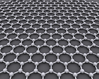
The schematic crystal structures of (a) ABA- and (b) ABC- stacked three layer graphene.
Graphene's carbon atoms are arranged into hexagons, forming a honeycomb-like lattice. Placing one layer of graphene on top of another leads to the formation of bilayer graphene. The layers can be arranged in one of two positions: the centres of the carbon hexagons of each layer can be organized immediately above one another, called AA-stacking, or they can be displaced forwards so that a hexagon centre in one layer is above a carbon atom below it, called AB-stacking. AB-stacking of two layers of graphene leads to the formation of a material with semiconducting properties by applying an external electric field.
Deliberately stacking three layers of graphene has proven difficult. But doing so could help researchers study how the physical properties of tri-layered materials change based on how the layers are stacked. This could lead to the development of novel electrical devices.
Researchers at Japan's Tohoku University and Nagoya University have now fabricated two different types of trilayer graphene with different electrical properties.
They heated silicon carbide using one of two methods. In one experiment, silicon carbide was heated to 1,510°C under pressurized argon. In another, it was heated to 1,300°C in a high vacuum. Both materials were then sprayed with hydrogen gas in which the bonds were broken to form single hydrogen atoms. Two types of trilayer graphene then formed. The silicon carbide heated under pressurized argon formed into ABA-stacked graphene, in which the hexagons of the top and bottom layers were exactly aligned while the middle layer was slightly displaced. The silicon carbide heated in a vacuum developed into ABC-stacked graphene, in which each layer was slightly displaced in front of the one below it.
The researchers then examined the physical properties of each material and found that their electrons behaved differently. The ABA graphene was an excellent electrical conductor, similar to monolayer graphene. The ABC grapheme, on the other hand, acts more like AB graphene in that it had semi-conductor properties.
"The present success in selective fabrication of ABA and ABC trilayer graphene would widen the feasibility of graphene-based nano-electronic devices with variable layer numbers and stacking sequences," conclude the researchers in their study published in the journal NPG Asia Materials.
Share on:


Suggested Items
SMC Korea 2024 to Highlight Semiconductor Materials Trends and Innovations on Industry’s Path to $1 Trillion
04/24/2024 | SEMIWith Korea a major consumer of semiconductor materials and advanced materials a key driver of innovation on the industry’s path to $1 trillion, industry leaders and experts will gather at SMC (Strategic Materials Conference) Korea 2024 on May 29 at the Suwon Convention Center in Gyeonggi-do, South Korea to provide insights into the latest materials developments and trends. Registration is open.
Groundbreaking Ceremony Marks the Beginning of a New Era for Newccess Industrial; The Construction of the MINGXIN Building
04/12/2024 | Newccess IndustrialOn a clear and sunny day in March, the groundbreaking ceremony for the MINGXIN Building took place in Shenzhen, China. This moment marked the official commencement of construction for a project that will reshape the semiconductor materials industry.
The Need for a Holistic Global Sustainability Standard
04/10/2024 | Michael Ford, Aegis SoftwareNo one can deny that the resources of our fragile planet are finite. The environment seems like a third party, subject to constant degradation. We’re acutely aware of the effects of pollution on our climate, and despite our “throw-away” culture, recycling and recovery of materials has remained relatively expensive, even as we use more energy just to survive.
iNEMI Publishes Four Roadmap Topics
04/04/2024 | iNEMIThe International Electronics Manufacturing Initiative (iNEMI) announces the availability of the first roadmap topics in the new iNEMI Roadmap format. Printed circuit boards, sustainable electronics, smart manufacturing, and mmWave materials and test are now available online.
Insulectro’s 'Storekeepers' Extend Their Welcome to Technology Village at IPC APEX EXPO
04/03/2024 | InsulectroInsulectro, the largest distributor of materials for use in the manufacture of PCBs and printed electronics, welcomes attendees to its TECHNOLOGY VILLAGE during this year’s IPC APEX EXPO at the Anaheim Convention Center, April 9-11, 2024.