


 It’s Only Common Sense: OCCAM—the Time Is Now
 Marcy's Musings: The Growing Industry
 Dan’s Biz Bookshelf: Seeing the How
Graphene Printing Technique 'Silk Screens' Flexible Electronics
October 22, 2018 | IEEEEstimated reading time: 4 minutes
Future high-efficiency solar cells molded to the surface of a car; ultra-small photonics chips; and low-power, long-lasting wearable devices will all require something no one’s yet been able to achieve, namely chips made from high-efficiency materials that are flexible, thin and inexpensive to manufacture.
A research group at MIT has announced a couple of developments in recent weeks that bring such a confluence of innovations closer to the achievable. Jeehwan Kim’s research group announced separately this month in Nature Materials and Science that they can inexpensively mass-produce ultra-thin gallium arsenide and gallium nitride chips as well as a harvest the monolayer materials necessary for manufacturing other 2-D electronics like tiny photonics devices.
“We [found] the way to go to expensive semiconducting materials so you can keep producing high-quality, high-performance semiconductors with a cheaper price,” says Kim, associate professor of mechanical engineering and materials science at MIT. “The bonus is you can have flexible semiconducting devices, and because they’re really thin, you can stack them up.”
As Spectrum reported last year, Kim’s group essentially uses graphene sheets as nano-sized silk screens through which expensively manufactured exotic material-based semiconductors can be laid down.
The recipe: Take a costly, manufactured, ultra-thin film of pure semiconducting material like gallium arsenide and lay a single-layered sheet of graphene on top of it. Then flow atoms of gallium and arsenide over the graphene, and the intermediary sheet acts as a surface on which an identical copy of the underlying ultra-thin film is copied on top of the graphene — although how and why the process worked as well as it did had previously been unclear.
In the current work, Kim’s group has expanded and generalized their previous finding — discovering that on one hand that single atom crystals like silicon cannot be replicated by the “silk screen” technique (what the group calls remote epitaxy) but on the other hand that practically any 2D sheet or film whose molecules carry any net electric polarity to them can be mass produced via remote epitaxy.
The reason, the group discovered, is that electrically the graphene behaves as if it’s not even there, transmitting the ionic electric fields from the 2D material up to the slurry of raw materials resting on top of the graphene. The fields then guide the slurry into forming a perfect duplicate of the expensively manufactured thin film below.
Kim uses the shorthand term “copy-paste” to describe the simple and seemingly inexpensive procedure as it’s now being developed. (He admits, however, he cannot give price quotes at the moment, because they haven’t yet done an economic analysis of the process.)
“We were able to copy-paste … through graphene for many types of compound materials in the periodic table,” says Kim. “That is a big discovery. Based on that understanding, we were able to make single-crystalline, free-standing, very very thin membrane compound materials.”
Kim says his research group is working with “six major companies” in Korea, Japan and the United States to scale up the ultra-thin chip manufacturing processes they’re developing. He expects some of these technologies might only need “a couple years” before they’re potentially ready for commercial application.
The industries and product lines Kim says could find use for the remote epitaxy process include solar energy (cheap but ultra-efficient GaAs solar panels have long been a dream), photonics (layering multiple ultra thin films on top of each other, say, that each are efficient at transmitting red LED light and blue LED light), wearables (making electronics ultra flexible but also low power is a holy grail in the field) and IoT (ditto).
The group has a portfolio of published results that includes the graphene remote epitaxy process. Also in the running is another 2D material manufacturing technique, the one published in Science.
“We developed a way to handle wafer-scale two-dimensional materials with atomic precision,” Kim says. The idea is other materials that could be useful as conductors, insulators and semiconductors may not necessarily work with the graphene method. In which case, Kim’s group has a second method for peeling off individual individual atom-thick monolayers.
As they spell out in the Science paper, they discovered that other ultra-thin films that may for various reasons not work as well with remote epitaxy could still be copied in another way. Compounds like hexagonal boron nitride (attractive as a lubricant, electrical insulator or light emitter) and tungsten disulfide (another possible post-silicon solar panel material) can be flaked off into single-atom thick sheets with a process Kim’s lab calls controlled crack propagation.
The process involves growing a thick material on a wafer and then attaching the top of that material to a nickel plate. (2D films adhere more strongly to nickel.) The nickel plate can then be pulled up, in the process exfoliating a single-atom layer thick of the target material. The exfoliated 2D film can then be laid down onto a host wafer as part of that wafer’s manufacturing process.
Arbitrarily many single-atom thick layers can be laid down this way, Kim says, leading to new kinds of electronic devices that demand complex semiconducting substrates.
“There has been no way of handling this one atom-thick layer controllably,” Kim says. “That’s why industry has not been discussing using 2D materials in next-generation electronics. [But] we can just grow thick 2D material on the wafer. Then we just peel off one monolayer, then one monolayer. We can harvest a lot of 2D materials from … the wafer.”
Between remote epitaxy and controlled crack propagation, Kim says many more flexible, efficient electronic, photonic and other thin-film based technologies can now be more reliably mass-produced.
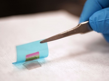
MIT researchers have devised a way to grow a single crystalline compound semiconductor on its substrate through two-dimensional materials. The compound semiconductor thin film is then exfoliated by a flexible substrate, showing the rainbow color that comes from thin film interference.
By Mark Anderson
Share on:


Suggested Items
SMC Korea 2024 to Highlight Semiconductor Materials Trends and Innovations on Industry’s Path to $1 Trillion
04/24/2024 | SEMIWith Korea a major consumer of semiconductor materials and advanced materials a key driver of innovation on the industry’s path to $1 trillion, industry leaders and experts will gather at SMC (Strategic Materials Conference) Korea 2024 on May 29 at the Suwon Convention Center in Gyeonggi-do, South Korea to provide insights into the latest materials developments and trends. Registration is open.
Groundbreaking Ceremony Marks the Beginning of a New Era for Newccess Industrial; The Construction of the MINGXIN Building
04/12/2024 | Newccess IndustrialOn a clear and sunny day in March, the groundbreaking ceremony for the MINGXIN Building took place in Shenzhen, China. This moment marked the official commencement of construction for a project that will reshape the semiconductor materials industry.
The Need for a Holistic Global Sustainability Standard
04/10/2024 | Michael Ford, Aegis SoftwareNo one can deny that the resources of our fragile planet are finite. The environment seems like a third party, subject to constant degradation. We’re acutely aware of the effects of pollution on our climate, and despite our “throw-away” culture, recycling and recovery of materials has remained relatively expensive, even as we use more energy just to survive.
iNEMI Publishes Four Roadmap Topics
04/04/2024 | iNEMIThe International Electronics Manufacturing Initiative (iNEMI) announces the availability of the first roadmap topics in the new iNEMI Roadmap format. Printed circuit boards, sustainable electronics, smart manufacturing, and mmWave materials and test are now available online.
Insulectro’s 'Storekeepers' Extend Their Welcome to Technology Village at IPC APEX EXPO
04/03/2024 | InsulectroInsulectro, the largest distributor of materials for use in the manufacture of PCBs and printed electronics, welcomes attendees to its TECHNOLOGY VILLAGE during this year’s IPC APEX EXPO at the Anaheim Convention Center, April 9-11, 2024.