


 It’s Only Common Sense: OCCAM—the Time Is Now
 Marcy's Musings: The Growing Industry
 Dan’s Biz Bookshelf: Seeing the How
Mass Manufacturing of Metasurfaces
March 18, 2019 | A*STAREstimated reading time: 1 minute
The mass production of flat optical devices with sub-wavelength structures could soon be a reality, thanks to a metasurface fabrication technique developed by researchers at A*STAR.
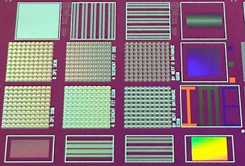
Image Caption: The metasurface's nano-pillar arrays displaying the letters I, M and E in red, green and blue, respectively. (The Optical Society)
Metasurfaces are synthetic, two-dimensional materials covered in tiny individual shapes with sizes and spacings smaller than the wavelengths of visible light. These ‘sub-wavelength’ structures enable scientists to precisely control the propagating shape, or wavefront, of light beams. As such, metasurfaces show promise for many applications from high-resolution imaging and color printing to controlling light polarization. Mass production of metasurfaces, however, has proven challenging, limited by the complexity of realizing such precise patterns.
Now, Ting Hu and his colleagues at A*STAR’s Institute of Microelectronics (IME) have developed a method of building silicon-based metasurfaces by introducing existing techniques from semiconductor fabrication. Their new metasurface design can produce high-resolution red-green-blue (RGB) color displays.
Until now, metasurfaces have mainly been fabricated via electron beam lithography (EBL), which is not applicable to mass production, as Hu explains:
“With EBL, the focused electron beam moves slowly, step by step, across the metasurface substrate. Metasurfaces with millions — possibly billions — of elements require a very long time to be patterned via EBL. We desired a faster and more efficient way of patternation.”
Hu and the team based their technique on ‘immersion lithography’, which has long been used to etch patterns on to electronic components. With multiple exposures, complex patterns can be built up. The researchers used ultraviolet-based (UV) lithography for initial patternation on to silicon substrates, followed by plasma etching to form the designs in small pixel blocks that were assembled into a 12-inch display surface (see image).
“Our UV lithography tool is a scanner, which can pattern a whole 12 inch wafer with designed devices within half an hour,” says Hu. “We designed the physical dimensions of the nano-pillar arrays of the metasurface to accurately display colors, with fantastic results, for example displaying the letters I, M and E in red, green and blue respectively.”
Hu and the team hope to optimize their design and improve the etching process to minimize losses induced by light scattering and defects in the nano-structure arrays. They are also making efforts to realize flat, lightweight ‘meta-lenses’ and dot projectors with potential uses in facial recognition technologies.
Share on:


Suggested Items
Inkjet Solder Mask ‘Has Arrived’
04/10/2024 | Pete Starkey, I-Connect007I was delighted to be invited to attend an interactive webinar entitled “Solder Mask Coating Made Easy with Additive Manufacturing,” hosted by SUSS MicroTec Netherlands in Eindhoven. The webinar was introduced and moderated by André Bodegom, managing director at Adeon Technologies, and the speakers were Mariana Van Dam, senior product manager PCB imaging solutions at AGFA in Belgium; Ashley Steers, sales manager at Electra Polymers in the UK; and Dr. Luca Gautero, product manager at SUSS MicroTec Netherlands.
NetVia Group Acquires Direct Imaging from Mivatek
04/09/2024 | Miva TechnologiesMiva Technologies is pleased to announce NetVia Group, Irving, TX has acquired a new Miva 2400NG Dual Tray Direct Imaging System with 30-micron capabilities for inner, outer and soldermask imaging.
Teledyne to Acquire Adimec
02/13/2024 | TeledyneTeledyne Technologies Incorporated announced that it has entered into an agreement to acquire Adimec Holding B.V. and its subsidiaries.
Real Time with... productronica 2023: MivaTek Global Advances Technology With High-res Imaging System
12/08/2023 | Real Time with...productronicaMivaTek's Brendan Hogan talks about how the company employs Digitally Adaptive Rasterization Technology (DART) in their high-res imaging equipment. He also shares how the blurred line between semiconductors and microelectronics is driving broader application of the imaging process.
Keysight Enables Validation of Arbe 4D Imaging Radar Chipset
11/30/2023 | Keysight Technologies, Inc.Keysight Technologies, Inc. announces that Arbe has selected the E8719A Radar Target Solution (RTS) to test the Arbe 4D imaging radar chipset for automotive applications.