


 Marcy's Musings: The Growing Industry
 It’s Only Common Sense: Here’s What To Do After IPC APEX EXPO 2024
 Dan’s Biz Bookshelf: Seeing the How
Economical Way to Produce High-Performance Thin Films for Electronics
April 12, 2019 | Missouri University of Science and TechnologyEstimated reading time: 2 minutes
Researchers at Missouri S&T have found an unprecedented, economical method for creating high-performance inorganic thin films, or “epitaxial” films, used in the manufacture of semiconductors for flexible electronics, LEDs and solar cells.
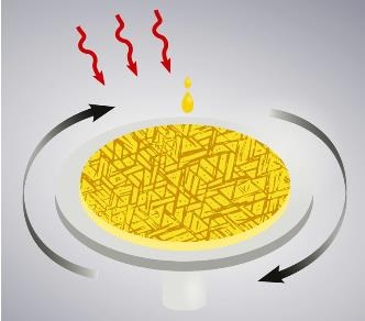
Schematic of spin coating process used to produce epitaxial films and nanocrystals. Image by Meagan V. Kelso.
“We’ve come up with a super-easy method that has never been done before to make these films from a solution using commercial spin coaters,” says Dr. Jay Switzer, the Donald L. Castleman/Foundation for Chemical Research Professor of Discovery in Chemistry at Missouri S&T. “This is an inexpensive and readily accessible route to single-crystal-like materials that should exhibit superior electronic and optical properties.
“In particular, our work with highly ordered epitaxial deposits of the perovskite material cesium lead bromide, a novel semiconductor used in highly efficient photovoltaic solar cells, stands to increase the efficiency of solar cells produced with this material,” Switzer adds.
Epitaxy is the growth of crystals, or thin films, whose orientation is determined by the crystalline substrate they are layered on. When the atomic structure of these crystals perfectly aligns with their substrate, the end result is a film with superior electronic and optical properties, rivaling the attributes of more expensive single crystals.
Electron and optical microscope images of epitaxial (A) cesium lead bromide, (B) lead iodide, (C) sodium chloride and (D) zinc oxide from Science 2019 DOI: 10.1126/science.aaw6184.
Until now, spin coating has been primarily used to make lithographic polymer coatings or to deposit organic semiconductor films on substrates, but the resulting films have been either polycrystalline or without crystalline structure — not epitaxial with the sought-after level of perfection needed for today’s state-of-the-art electronics.
“We’ve learned to use spin coating to make highly oriented films and nanocrystals on a variety of inorganic substrates,” says Switzer. “Until now, atomically perfect epitaxial films have been made by several other methods, and some of those are very expensive and require ultra-high vacuum.”
Those methods include molecular beam epitaxy (MBE), chemical vapor deposition, liquid-phase epitaxy, hydrothermal processing, chemical bath deposition and electrodeposition. According to the Small Business Innovation Research (SBIR) program, MBE machines cost about $1 million and much more for larger production systems; and Switzer says, each MBE machine must be dedicated to only one material. Other epitaxial methods are limited by high temperature and pressure requirements.
Over a two-year period, the research team showed that epitaxial films of inorganic materials such as lead iodide, zinc oxide, sodium chloride and perovskite crystal structures could be deposited on single crystals or comparable substrates by simply spin coating their solutions or precursors of the materials.
Switzer’s work bridges the gap between chemistry and materials science and integrates the efforts of graduate, undergraduate and sometimes high school students from both fields into his research team. The additional authors of this study are all from Missouri S&T and include Meagan Kelso and Naveen Mahenderkar, graduate students in materials science and engineering; Qingzhi Chen, a graduate student in chemistry; and John Tubbesing, a senior in chemistry.
Switzer holds 13 U.S. patents, primarily focused on the electrodeposition of functional materials. He is a fellow of the Electrochemical Society, the American Association for the Advancement of Science, the Materials Research Society, and the Japan Society for the Promotion of Science.
Share on:


Suggested Items
Fineline Global Group Acquires IBR
04/19/2024 | PRNewswireIBR Leiterplatten GmbH & Co. KG joins the Fineline Global Group and is now an integral part of one of the leading suppliers of PCBs. Fine Line Gesellschaft für Leiterplattentechnik mbH acquired 100% shares of IBR.
SEMI Applauds U.S. Chips Act Award for Samsung Electronics Facilities to Strengthen Domestic Semiconductor Supply Chain
04/17/2024 | SEMISEMI, the industry association serving the global electronics design and manufacturing supply chain, applauded the United States Department of Commerce’s announcement of a Preliminary Memorandum of Terms for an award under the CHIPS and Science Act to support the expansion of Samsung Electronics’ presence in Texas and the company’s development and production of leading-edge chips.
Microchip Technology Expands Partnership with TSMC to Strengthen Semiconductor Manufacturing Capacity
04/08/2024 | Microchip Technology Inc.Microchip Technology announced it has expanded its partnership with TSMC, the world’s leading semiconductor foundry, to enable a specialized 40 nm manufacturing capacity at Japan Advanced Semiconductor Manufacturing, Inc. (JASM), TSMC’s majority-owned manufacturing subsidiary in Kumamoto Prefecture, Japan.
MS2 a Beneficial System for Reducing Solder Dross
04/04/2024 | I-Connect007 Editorial TeamWe recently spoke with Octavio Raygoza, sales manager for P.Kay Metal in Mexico, to discuss how P.Kay’s MS2® system for reducing solder dross is both financially and environmentally responsible. By reducing solder dross up to 85%, you nearly double the output while consuming the same amount of solder.
Hentec/RPS to Exhibit Vector Selective Soldering and Odyssey Lead Tinning Systems at IPC APEX EXPO 2024
04/04/2024 | Hentec Industries/RPS AutomationHentec Industries/RPS Automation, a leading manufacturer of selective soldering, lead tinning and solderability testing equipment, is pleased to announce it will exhibit its Vector 300 selective soldering and Odyssey 925 lead tinning systems at the upcoming IPC EXPO 2024.