


 It’s Only Common Sense: OCCAM—the Time Is Now
 Marcy's Musings: The Growing Industry
 Dan’s Biz Bookshelf: Seeing the How
Seeing Infrared: Sandia’s Nanoantennas Help Detectors See More Heat, Less Noise
September 17, 2019 | Sandia National LaboratoriesEstimated reading time: 3 minutes
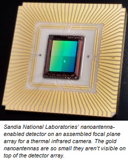
Sandia National Laboratories researchers have developed tiny, gold antennas to help cameras and sensors that “see” heat deliver clearer pictures of thermal infrared radiation for everything from stars and galaxies to people, buildings and items requiring security.
In a Laboratory Directed Research and Development project, a team of researchers developed a nanoantenna-enabled detector that can boost the signal of a thermal infrared camera by up to three times and improve image quality by reducing dark current, a major component of image noise, by 10 to 100 times.
Thermal infrared cameras and sensors have existed for 50 years, but the traditional design of the detector that sits behind the camera lens or a sensor’s optical system seems to be reaching its performance limits, said David Peters, a Sandia manager and nanoantenna project lead.
He said improved sensitivity in infrared detectors, beyond what the typical design can deliver, is important for both Sandia’s national security work and for other uses, such as astronomical research.
Seeing More with Less
The sensitivity and image quality of an infrared detector usually depends on a thick layer of detector material that absorbs incoming heat and turns it into an electrical signal that can be collected and turned into an image. The thickness of the detector layer determines how much heat can be absorbed and read by the camera, but thick layers also have drawbacks.
“The detector material is always spontaneously creating electrons that are collected and add noise to the image, which reduces image quality,” Peters said. “This phenomenon, called dark current, increases along with the thickness of the detector material — the thicker the material is, the more noise in the image it creates.”
The research team developed a new detector design that breaks away from relying on thick layers and instead uses a subwavelength nanoantenna, a patterned array of gold square or cross shapes, to concentrate the light on a thinner layer of detector material. This design uses just a fraction of a micron of detector material, whereas traditional thermal infrared detectors have a thickness of 5 to 10 microns. A human hair is about 75 microns in width.
The nanoantenna-enhanced design helps detectors see more than 50% of an object’s infrared radiation while also reducing image distortion caused by dark current, whereas current technology can only see about 25% of infrared radiation. It also allows for the invention of new detector concepts that are not possible with existing technology.
“For example, with nanoantennas, it’s possible to dramatically expand the amount of information acquired in an image by exquisitely controlling the spectral response at the pixel level,” Peters said.
The team makes the nanoantenna-enabled detectors by slightly altering the usual process for making an infrared detector. It starts by “growing” the detector material on top of a thin disk called a wafer. Then the detector material is flipped onto a layer of electronics that read the signals collected by the nanoantenna and the detector layer. After discarding the wafer, a tiny amount of gold is applied to create the patterned nanoantenna layer on top of the detector material.
From National Lab to Industry
“It was not a given that this was going to work, so that’s why Sandia took it on,” Peters said. “Now, we are to the point where we have proven this concept and this technology is ready to be commercialized. This concept can be applied to different detector types, so there’s an opportunity for existing manufacturers to integrate this new technology with their existing detectors.”
Peters said Sandia is pursuing leads to establish a Collaborative Research and Development Agreement to start transferring the technology to industry.
“This project is a perfect example of how a national lab can prove a concept and then spin it off to industry where it can be developed further,” Peters said.
This research was conducted at Sandia’s National Security Photonics Center. For more information about Sandia’s work in developing and delivering integrated photonics solutions for national security applications, visit the center’s website.
About Sandia National Laboratories
Sandia National Laboratories is a multimission laboratory operated by National Technology and Engineering Solutions of Sandia LLC, a wholly owned subsidiary of Honeywell International Inc., for the U.S. Department of Energy’s National Nuclear Security Administration. Sandia Labs has major research and development responsibilities in nuclear deterrence, global security, defense, energy technologies and economic competitiveness, with main facilities in Albuquerque, New Mexico, and Livermore, California.
Share on:


Suggested Items
Designer’s Notebook: What Designers Need to Know About Manufacturing, Part 2
04/24/2024 | Vern Solberg -- Column: Designer's NotebookThe printed circuit board (PCB) is the primary base element for providing the interconnect platform for mounting and electrically joining electronic components. When assessing PCB design complexity, first consider the component area and board area ratio. If the surface area for the component interface is restricted, it may justify adopting multilayer or multilayer sequential buildup (SBU) PCB fabrication to enable a more efficient sub-surface circuit interconnect.
Happy’s Tech Talk #27: Integrated Mesh Power System (IMPS) for PCBs
04/08/2024 | Happy Holden -- Column: Happy’s Tech TalkA significant decrease in HDI substrate production cost can be achieved by reducing the number of substrate layers from conventional through-hole multilayers and microvia multilayers of eight, 10, 12, and more to only two layers. Besides reducing direct processing steps, the yield will increase as defect-producing operations are eliminated. The integrated mesh power system (IMPS) was invented in the latter years of MCM-D use for thin-film fabrication. Those geometries fit today into our use of ultra HDI.
Insulectro’s 'Storekeepers' Extend Their Welcome to Technology Village at IPC APEX EXPO
04/03/2024 | InsulectroInsulectro, the largest distributor of materials for use in the manufacture of PCBs and printed electronics, welcomes attendees to its TECHNOLOGY VILLAGE during this year’s IPC APEX EXPO at the Anaheim Convention Center, April 9-11, 2024.
Now Available: Episode 4, Season 2 of Designing for Reality—Lamination
04/04/2024 | I-Connect007I-Connect007 has just released the latest episode of its podcast series, On the Line With..., which focuses on designing for reality in the electronics industry. Multilayer boards bring along a completely different set of processes. In this installment, ASC Sunstone VP/Manager Matt Stevenson discusses manufacturing techniques for multilayer boards. Of course, this necessitates a review of drill and registration techniques, followed by the ins and outs of lamination.
Heavy Copper PCBs: Bridging the Gap Between Design and Fabrication, Part 1
04/01/2024 | Yash Sutariya, Saturn Electronics ServicesThey call me Sparky. This is due to my talent for getting shocked by a variety of voltages and because I cannot seem to keep my hands out of power control cabinets. While I do not have the time to throw the knife switch to the off position, that doesn’t stop me from sticking screwdrivers into the fuse boxes. In all honesty, I’m lucky to be alive. Fortunately, I also have a talent for building high-voltage heavy copper circuit boards. Since this is where I spend most of my time, I can guide you through some potential design for manufacturability (DFM) hazards you may encounter with heavy copper design.