


 It’s Only Common Sense: OCCAM—the Time Is Now
 Marcy's Musings: The Growing Industry
 Dan’s Biz Bookshelf: Seeing the How
Energy Efficient Power Electronics—Gallium Oxide Power Transistors with Record Levels
October 2, 2019 | FBHEstimated reading time: 1 minute
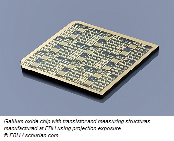
With as little space as possible, they should be able to achieve ever higher power densities with low energy consumption and thus work more efficiently. Conventional components reach their limits here. As a result, scientists around the world are researching novel materials and components that meet these requirements. The Ferdinand Braun Institute, Leibniz Institute for High Frequency Technology (FBH) has now achieved a breakthrough with transistors based on gallium oxide (ß-Ga2O3).
The newly developed ß-Ga2O3 MOSFETs (dt. Metal-oxide-semiconductor field effect transistor) provide a high breakdown voltage with high current conductivity. With 1.8 kilovolts of breakdown voltage and a record output of 155 megawatts per square centimeter, they achieve unique global metrics close to the theoretical material limit of gallium oxide. At the same time, the breakthrough field strengths achieved are far greater than those of established large band gap semiconductors such as silicon carbide or gallium nitride.
Optimized layer structure and gate topology
To achieve these improvements, the FBH team started on the layer structure and the gate topology. The basis was provided by substrates from the Leibniz Institute for Crystal Growth (IKZ) with an optimized epitaxial layer structure. This reduced the defect density and improved the electrical properties. This leads to lower resistances when switched on. The gate is the central "switching point" in field effect transistors, which is controlled by the gate-source voltage. Its topology has been further developed so that the high field strengths at the gate edge could be reduced. This in turn leads to higher breakdown voltages.
Share on:


Suggested Items
Happy’s Tech Talk #27: Integrated Mesh Power System (IMPS) for PCBs
04/08/2024 | Happy Holden -- Column: Happy’s Tech TalkA significant decrease in HDI substrate production cost can be achieved by reducing the number of substrate layers from conventional through-hole multilayers and microvia multilayers of eight, 10, 12, and more to only two layers. Besides reducing direct processing steps, the yield will increase as defect-producing operations are eliminated. The integrated mesh power system (IMPS) was invented in the latter years of MCM-D use for thin-film fabrication. Those geometries fit today into our use of ultra HDI.
Insulectro’s 'Storekeepers' Extend Their Welcome to Technology Village at IPC APEX EXPO
04/03/2024 | InsulectroInsulectro, the largest distributor of materials for use in the manufacture of PCBs and printed electronics, welcomes attendees to its TECHNOLOGY VILLAGE during this year’s IPC APEX EXPO at the Anaheim Convention Center, April 9-11, 2024.
Now Available: Episode 4, Season 2 of Designing for Reality—Lamination
04/04/2024 | I-Connect007I-Connect007 has just released the latest episode of its podcast series, On the Line With..., which focuses on designing for reality in the electronics industry. Multilayer boards bring along a completely different set of processes. In this installment, ASC Sunstone VP/Manager Matt Stevenson discusses manufacturing techniques for multilayer boards. Of course, this necessitates a review of drill and registration techniques, followed by the ins and outs of lamination.
Heavy Copper PCBs: Bridging the Gap Between Design and Fabrication, Part 1
04/01/2024 | Yash Sutariya, Saturn Electronics ServicesThey call me Sparky. This is due to my talent for getting shocked by a variety of voltages and because I cannot seem to keep my hands out of power control cabinets. While I do not have the time to throw the knife switch to the off position, that doesn’t stop me from sticking screwdrivers into the fuse boxes. In all honesty, I’m lucky to be alive. Fortunately, I also have a talent for building high-voltage heavy copper circuit boards. Since this is where I spend most of my time, I can guide you through some potential design for manufacturability (DFM) hazards you may encounter with heavy copper design.
Kioxia, WD Elevate Capacity Utilization, Pushing NAND Flash Supply Growth to 10.9%
03/19/2024 | TrendForceTrendForce reports that anticipation of NAND Flash price hikes into Q2 has motivated certain suppliers to minimize losses and lower costs in hopes of returning to profitability this year.