


 It’s Only Common Sense: OCCAM—the Time Is Now
 Marcy's Musings: The Growing Industry
 Dan’s Biz Bookshelf: Seeing the How
Powering the Future: Smallest All-Digital Circuit Opens Doors to 5 NM Next-Gen Semiconductor
February 10, 2020 | Tokyo Institute of Technology, Socionext Inc.Estimated reading time: 3 minutes
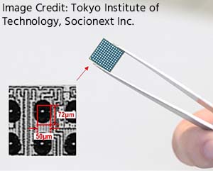
Scientists at Tokyo Institute of Technology (Tokyo Tech) and Socionext Inc. have designed the world's smallest all-digital phase-locked loop (PLL). PLLs are critical clocking circuits in virtually all digital applications, and reducing their size and improving their performance is a necessary step to enabling the development of next-generation technologies.
New or improved technologies, such as artificial intelligence, 5G cellular communications, and the Internet-of-Things, are expected to bring revolutionary changes in society. But for that to happen, high-performance system-on-a-chip (SoC)—a type of integrated circuit—devices are indispensable. A core building block of SoC devices is the phase-locked loop (PLL), a circuit that synchronizes with the frequency of a reference oscillation and outputs a signal with the same or higher frequency. PLLs generate 'clocking signals', whose oscillations act as a metronome that provides a precise timing reference for the harmonious operation of digital devices.
For high performance SoC devices to be realized, fabrication processes for semiconductor electronics must become more sophisticated. The smaller the area to implement digital circuitry is, the better the performance of the device. Manufacturers have been racing to develop increasingly smaller semiconductors. 7 nm semiconductors (a massive improvement over their 10 nm predecessor) are already in production, and methods to build 5 nm ones are now being looked at.
However, in this endeavor stands a major bottleneck. Existing PLLs require analog components, which are generally bulky and have designs that are difficult to scale down.
Scientists at Tokyo Tech and Socionext Inc., led by Prof. Kenichi Okada, have addressed this issue by implementing a 'synthesizable' fractional-N PLL, which only requires digital logic gates, and no bulky analog components, making it easy to adopt in conventional miniaturized integrated circuits.
Okada and team used several techniques to decrease the required area, power consumption and jitter—unwanted time fluctuations when transmitting digital signals—of their synthesizable PLLs. To decrease area, they employed a ring oscillator, a compact oscillator that can be easily scaled down. To suppress jitter, they reduced the phase noise—random fluctuations in a signal—of this ring oscillator, using 'injection locking'—the process of synchronizing an oscillator with an external signal whose frequency (or multiple of it) is close to that of the oscillator—over a wide range of frequencies. The lower phase noise, in turn, reduced power consumption.
The design of this synthesizable PLL beats that of all other current state-of-the-art PLLs in many important aspects. It achieves the best jitter performance with the lowest power consumption and smallest area (as can be seen in Figure 1). "The core area is 0.0036 mm2, and the whole PLL is implemented as one layout with a single power supply," remarks Okada. Further, it can be built using standard digital design tools, allowing for its rapid, low-effort, and low-cost production, making it commercially viable.
This synthesizable PLL can be easily integrated into the design of all-digital SoCs, and is commercially viable, making it valuable for developing the much sought after 5 nm semiconductor for cutting-edge applications including artificial intelligence, internet of things and many others, where high performance and low power consumption would be the critical requirements. But the contributions of this research go beyond these possibilities. "Our work demonstrates the potential of synthesizable circuits. With the design methodology employed here, other building blocks of SoCs, such as data converters, power management circuits, and wireless transceivers, could be made synthesizable as well. This would greatly boost design productivity and considerably reduce design efforts," explains Okada. Tokyo Tech and Socionext will continue their collaboration in this filed to advance the miniaturization of electronic devices, enabling the realization of newer-generation technologies.
This research work was conducted in cooperation with TeraPixel Technologies Inc.
Share on:


Suggested Items
Cadence, TSMC Collaborate on Wide-Ranging Innovations to Transform System and Semiconductor Design
04/25/2024 | Cadence Design SystemsCadence Design Systems, Inc. and TSMC have extended their longstanding collaboration by announcing a broad range of innovative technology advancements to accelerate design, including developments ranging from 3D-IC and advanced process nodes to design IP and photonics.
Ansys, TSMC Enable a Multiphysics Platform for Optics and Photonics, Addressing Needs of AI, HPC Silicon Systems
04/25/2024 | PRNewswireAnsys announced a collaboration with TSMC on multiphysics software for TSMC's Compact Universal Photonic Engines (COUPE). COUPE is a cutting-edge Silicon Photonics (SiPh) integration system and Co-Packaged Optics platform that mitigates coupling loss while significantly accelerating chip-to-chip and machine-to-machine communication.
Siemens’ Breakthrough Veloce CS Transforms Emulation and Prototyping with Three Novel Products
04/24/2024 | Siemens Digital Industries SoftwareSiemens Digital Industries Software launched the Veloce™ CS hardware-assisted verification and validation system. In a first for the EDA (Electronic Design Automation) industry, Veloce CS incorporates hardware emulation, enterprise prototyping and software prototyping and is built on two highly advanced integrated circuits (ICs) – Siemens’ new, purpose-built Crystal accelerator chip for emulation and the AMD Versal™ Premium VP1902 FPGA adaptive SoC (System-on-a-chip) for enterprise and software prototyping.
Listen Up! The Intricacies of PCB Drilling Detailed in New Podcast Episode
04/25/2024 | I-Connect007In episode 5 of the podcast series, On the Line With: Designing for Reality, Nolan Johnson and Matt Stevenson continue down the manufacturing process, this time focusing on the post-lamination drilling process for PCBs. Matt and Nolan delve into the intricacies of the PCB drilling process, highlighting the importance of hole quality, drill parameters, and design optimization to ensure smooth manufacturing. The conversation covers topics such as drill bit sizes, aspect ratios, vias, challenges in drilling, and ways to enhance efficiency in the drilling department.
Elevating PCB Design Engineering With IPC Programs
04/24/2024 | Cory Blaylock, IPCIn a monumental stride for the electronics manufacturing industry, IPC has successfully championed the recognition of the PCB Design Engineer as an official occupation by the U.S. Department of Labor (DOL). This pivotal achievement not only underscores the critical role of PCB design engineers within the technology landscape, but also marks the beginning of a transformative journey toward nurturing a robust, skilled workforce ready to propel our industry into the future.