


 It’s Only Common Sense: OCCAM—the Time Is Now
 Marcy's Musings: The Growing Industry
 Dan’s Biz Bookshelf: Seeing the How
Quik-Pak Announces Substrate Development Service
February 11, 2020 | Quik-PakEstimated reading time: 1 minute
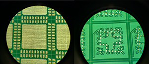
Quik-Pak, a provider of innovative microelectronic packaging and assembly solutions, today announced its substrate design, fabrication and assembly service. Utilizing virtually any substrate type, Quik-Pak can create turnkey solutions for substrate-based assemblies to accommodate customers’ unique packaging requirements, with delivery times at least 50% faster than those of competitive services.
Quik-Pak’s substrate service targets both ICs and MEMS, and its ability to accommodate all types of substrates provides engineering flexibility that allows greater design freedom for a wide range of advanced packages. Quik-Pak has offered this capability, in a limited fashion, for several years. Its success has spurred the company to step up activity—particularly in the face of broadening demand for custom packaging solutions that can fill the gaps not met by standard, off-the-shelf packages.
One key driver for this demand is the increased need for custom RF packages in the face of 5G’s imminent rollout. Technologies in which Quik-Pak specializes, such as laminate quad flat no-lead (QFN) and organic QFN for flip-chips, are well suited to integration and customization. The service can also accommodate 3D packaging, ball grid arrays (BGAs), systems-in-package (SiPs) and multichip modules (MCMs).
According to Quik-Pak Chief Operating Officer Ken Molitor, “We can tune our process to optimize the customer’s desired parameter—size, performance, application—creating a solution in about five weeks, from initial consultation to finished assembly. Other services can take five weeks to complete the design alone and up to 16 weeks to deliver the assembled package. With this combination of quality and speed, Quik-Pak is poised to broaden the reach of our service to address new markets and applications, such as military, medical, sensors and other custom arenas.”
Quik-Pak will be showcasing its full range of capabilities, including its new substrate service offering, in the expo hall at the 16th annual IMAPS International Conference on Device Packaging. The company is also a sponsor of the event, to be held March 2-5, 2020, in Fountain Hills, Ariz.
Share on:


Suggested Items
Cadence, TSMC Collaborate on Wide-Ranging Innovations to Transform System and Semiconductor Design
04/25/2024 | Cadence Design SystemsCadence Design Systems, Inc. and TSMC have extended their longstanding collaboration by announcing a broad range of innovative technology advancements to accelerate design, including developments ranging from 3D-IC and advanced process nodes to design IP and photonics.
Ansys, TSMC Enable a Multiphysics Platform for Optics and Photonics, Addressing Needs of AI, HPC Silicon Systems
04/25/2024 | PRNewswireAnsys announced a collaboration with TSMC on multiphysics software for TSMC's Compact Universal Photonic Engines (COUPE). COUPE is a cutting-edge Silicon Photonics (SiPh) integration system and Co-Packaged Optics platform that mitigates coupling loss while significantly accelerating chip-to-chip and machine-to-machine communication.
Siemens’ Breakthrough Veloce CS Transforms Emulation and Prototyping with Three Novel Products
04/24/2024 | Siemens Digital Industries SoftwareSiemens Digital Industries Software launched the Veloce™ CS hardware-assisted verification and validation system. In a first for the EDA (Electronic Design Automation) industry, Veloce CS incorporates hardware emulation, enterprise prototyping and software prototyping and is built on two highly advanced integrated circuits (ICs) – Siemens’ new, purpose-built Crystal accelerator chip for emulation and the AMD Versal™ Premium VP1902 FPGA adaptive SoC (System-on-a-chip) for enterprise and software prototyping.
Listen Up! The Intricacies of PCB Drilling Detailed in New Podcast Episode
04/25/2024 | I-Connect007In episode 5 of the podcast series, On the Line With: Designing for Reality, Nolan Johnson and Matt Stevenson continue down the manufacturing process, this time focusing on the post-lamination drilling process for PCBs. Matt and Nolan delve into the intricacies of the PCB drilling process, highlighting the importance of hole quality, drill parameters, and design optimization to ensure smooth manufacturing. The conversation covers topics such as drill bit sizes, aspect ratios, vias, challenges in drilling, and ways to enhance efficiency in the drilling department.
Elevating PCB Design Engineering With IPC Programs
04/24/2024 | Cory Blaylock, IPCIn a monumental stride for the electronics manufacturing industry, IPC has successfully championed the recognition of the PCB Design Engineer as an official occupation by the U.S. Department of Labor (DOL). This pivotal achievement not only underscores the critical role of PCB design engineers within the technology landscape, but also marks the beginning of a transformative journey toward nurturing a robust, skilled workforce ready to propel our industry into the future.