


 Happy’s Tech Talk #28: The Power Mesh Architecture for PCBs
 It’s Only Common Sense: Would You Join Your Own Company?
 The Chemical Connection: Reducing Etch System Water Usage, Part 2
A Tough Coat for Silicon
March 22, 2017 | A*STAREstimated reading time: 2 minutes
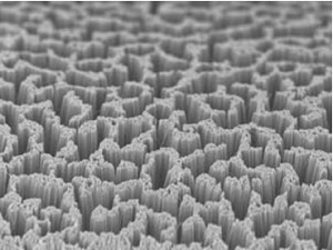
A simple, green method that applies a protective coating to semiconductors could help to develop these materials for many applications, from batteries to biosensors.
Silicon forms an oxide layer on its surface when exposed to air or moisture, which can detract from its electronic properties. Adding a ‘skin’ of molecules to the silicon can provide a physical barrier that prevents oxidation, but forming these monolayers can be tricky, requiring an inert atmosphere and long processing times, or demand the use of potentially harmful organic solvents.
Sreenivasa Reddy Puniredd of the A*STAR Institute of Materials Research and Engineering and colleagues have now developed a new way to deliver the protective molecules using supercritical carbon dioxide (scCO2). Carbon dioxide is converted to scCO2 under high pressure, when it becomes a free-flowing liquid that is chemically inert, inexpensive, and more environmentally-friendly than traditional solvents.
The researchers used scCO2 to carry molecules called alkylthiols, which contain long carbon chains with a sulfur atom at one end. Sulfur forms a stable bond with silicon, while the water-repelling carbon chains make a tightly-packed skin on silicon’s surface.
To apply the coating they used alkylthiols containing between seven and 18 carbon atoms to coat silicon, germanium, and silicon nanowires. Each procedure took a few hours, and produced monolayers between 1.6 nanometers and 2.3 nanometers thick that resisted wear and repelled water. The greatest effect was seen for the longest alkylthiol chains.
The monolayers also protected the surface from oxygen for more than 50 days; those prepared using conventional solvents were typically stable for less than seven days. “The increase in stability was expected, but such long-term stability was a surprise,” says Puniredd.
Silicon nanowires are being tested for a range of biological applications, including biosensors and antibacterial surfaces. Although fragile and easily damaged by other monolayer formation methods, the silicon nanowires were undamaged by the scCO2 process, allowing the researchers to test how they interacted with human liver cells. Those protected by the 18-carbon alkylthiol significantly reduced cell growth on the nanowires, compared with unprotected nanowires or a flat silicon surface. This is probably because the cells’ proteins could not latch on to the monolayer’s long carbon chains.
“This scCO2 technology can be adopted for many kinds of inorganic surface modification,” says Puniredd. “The technology is not only scalable, but also enhances the quality and stability of the film. It can potentially replace billions of pounds of organic solvents used every year in thin-film fabrication and cleaning applications.”
Share on:


Suggested Items
Real Time with… IPC APEX EXPO 2024: Exploring the Future of Surface Finishes
04/25/2024 | Real Time with...IPC APEX EXPOJoe McGurran, product marketing director for MKS Atotech, looks into the future of surface finishes, discussing less nickel, reduced thickness, technologies influencing HDI and UHDI, and the benefits of nickel-free surface finishes. He also touches on popular finishes like ENIG and palladium immersion gold and discusses the value proposition of making a change.
Designer’s Notebook: What Designers Need to Know About Manufacturing, Part 2
04/24/2024 | Vern Solberg -- Column: Designer's NotebookThe printed circuit board (PCB) is the primary base element for providing the interconnect platform for mounting and electrically joining electronic components. When assessing PCB design complexity, first consider the component area and board area ratio. If the surface area for the component interface is restricted, it may justify adopting multilayer or multilayer sequential buildup (SBU) PCB fabrication to enable a more efficient sub-surface circuit interconnect.
IDTechEx Report Unveils 3D Electronics Status and Opportunities
04/22/2024 | PRNewswire3D electronics is an emerging manufacturing approach that enables electronics to be integrated within or onto the surface of objects. 3D electronic manufacturing techniques empower new features, including mass customizability, greater integration, and improved sustainability in the electronics industry.
NASA, Japan Advance Space Cooperation, Sign Agreement for Lunar Rover
04/11/2024 | NASANASA Administrator Bill Nelson and Japan’s Minister of Education, Culture, Sports, Science and Technology (MEXT) Masahito Moriyama have signed an agreement to advance sustainable human exploration of the Moon.
Lockheed Martin Conducts Historic LRASM Flight Test
04/04/2024 | Lockheed MartinThe U.S. Navy in partnership with Lockheed Martin [NYSE: LMT] successfully conducted a historic Long-Range Anti-Ship Missile (LRASM) flight test with four missiles simultaneously in flight.