


 Material Insight: The Dielectric Constant of PCB Materials
 American Made Advocacy: What About the Rest of the Technology Stack?
 It’s Only Common Sense: Great Ideas From John Mitchell’s Book on Hiring Habits
Using Artificial Intelligence to Engineer Materials’ Properties
February 12, 2019 | MITEstimated reading time: 6 minutes
Applying just a bit of strain to a piece of semiconductor or other crystalline material can deform the orderly arrangement of atoms in its structure enough to cause dramatic changes in its properties, such as the way it conducts electricity, transmits light, or conducts heat.
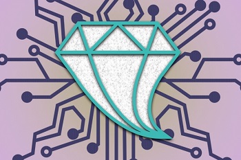
Image caption: Introducing a small amount of strain into crystalline materials, such as diamond or silicon, can produce significant changes in their properties, researchers have found. The mechanical strain is represented here as a deformation in the diamond's shape. Image: Chelsea Turner, MIT
Now, a team of researchers at MIT and in Russia and Singapore have found ways to use artificial intelligence to help predict and control these changes, potentially opening up new avenues of research on advanced materials for future high-tech devices.
The findings appear this week in the Proceedings of the National Academy of Sciences, in a paper authored by MIT professor of nuclear science and engineering and of materials science and engineering Ju Li, MIT Principal Research Scientist Ming Dao, and MIT graduate student Zhe Shi, with Evgeni Tsymbalov and Alexander Shapeev at the Skolkovo Institute of Science and Technology in Russia, and Subra Suresh, the Vannevar Bush Professor Emeritus and former dean of engineering at MIT and current president of Nanyang Technological University in Singapore.
Already, based on earlier work at MIT, some degree of elastic strain has been incorporated in some silicon processor chips. Even a 1% change in the structure can in some cases improve the speed of the device by 50%, by allowing electrons to move through the material faster.
Recent research by Suresh, Dao, and Yang Lu, a former MIT postdoc now at City University of Hong Kong, showed that even diamond, the strongest and hardest material found in nature, can be elastically stretched by as much as 9% without failure when it is in the form of nanometer-sized needles. Li and Yang similarly demonstrated that nanoscale wires of silicon can be stretched purely elastically by more than 15%. These discoveries have opened up new avenues to explore how devices can be fabricated with even more dramatic changes in the materials’ properties.
Strain Made to Order
Unlike other ways of changing a material’s properties, such as chemical doping, which produce a permanent, static change, strain engineering allows properties to be changed on the fly. “Strain is something you can turn on and off dynamically,” Li says.
But the potential of strain-engineered materials has been hampered by the daunting range of possibilities. Strain can be applied in any of six different ways (in three different dimensions, each one of which can produce strain in-and-out or sideways), and with nearly infinite gradations of degree, so the full range of possibilities is impractical to explore simply by trial and error. “It quickly grows to 100 million calculations if we want to map out the entire elastic strain space,” Li says.
Page 1 of 3
Share on:


Suggested Items
Material Insight: The Dielectric Constant of PCB Materials
05/17/2024 | Dr. Preeya Kuray -- Column: Material InsightIn the world of PCB design, miniaturization can be achieved by using low dielectric constant (Dk) materials. Low Dk materials can allow for a reduction in thickness while maintaining a given trace width, leading to lower transmission loss and higher density circuitry.
IPC APEX EXPO: Some Thoughts About Growth
05/16/2024 | Dan Feinberg, I-Connect007After two and a half days of wandering the aisles at IPC APEX EXPO 2024, for the first time, I almost felt like I was exploring CES. There were so many booths and exhibits that I could describe, but I’d like to focus on the growth and huge value of this event, which has expanded well beyond just the growing and impressive exhibit show floor.
The Shaughnessy Report: Unlock Your High-speed Material Constraints
05/15/2024 | Andy Shaughnessy -- Column: The Shaughnessy ReportThe world of PCB materials used to be a fairly simple one. It was divided into two groups: the “traditional” laminates, often called FR-4, and the high-speed laminates developed especially for high-speed PCBs. These were two worlds that usually didn’t collide. But then traditional laminates started getting better, and high-speed designers and design engineers took notice and started to reconsider what FR-4 could be used for.
Breaking High-speed Material Constraints: Design007 Magazine — May 2024
05/14/2024 | I-Connect007 Editorial TeamDo you need specialty materials for your high-speed designs? Maybe not. Improvements in resins mean designers of high-speed boards can sometimes use traditional laminate systems instead of high-speed materials, saving time and money while streamlining the fab process. In the May 2024 issue of Design007 Magazine, our contributors explain how to avoid overconstraining your materials when working with high-speed boards.
Indium Experts to Present at Electronics in Harsh Environments SMTA Conference
05/13/2024 | Indium Corporationndium Corporation Technical Manager for Europe, Africa, and the Middle East, Karthik Vijay, will deliver a technical presentation and Indium Corporation Senior Technologist, Dr. Ronald Lasky, will deliver both a workshop and technical presentation at the Electronics in Harsh Environments SMTA Conference on May 14-16 in Copenhagen, Denmark.