


 Material Insight: The Dielectric Constant of PCB Materials
 American Made Advocacy: What About the Rest of the Technology Stack?
 It’s Only Common Sense: Great Ideas From John Mitchell’s Book on Hiring Habits
Controlling Superconducting Regions within an Exotic Metal
October 11, 2019 | EPFLEstimated reading time: 2 minutes
Researchers at EPFL have created a metallic microdevice in which they can define and tune patterns of superconductivity. Their discovery, which holds great promise for quantum technologies of the future, has just been published in Science.
Superconductivity has fascinated scientists for many years since it offers the potential to revolutionize current technologies. Materials only become superconductors—meaning that electrons can travel in them with no resistance—at very low temperatures. These days, this unique zero resistance superconductivity is commonly found in a number of technologies, such as magnetic resonance imaging (MRI). Future technologies, however, will harness the total synchrony of electronic behavior in superconductors—a property called the phase. There is currently a race to build the world’s first quantum computer, which will use these phases to perform calculations. Conventional superconductors are very robust and hard to influence, and the challenge is to find new materials in which the superconducting state can be easily manipulated in a device.
EPFL’s Laboratory of Quantum Materials (QMAT), headed by Philip Moll, professor at the School of Engineering, has been working on a specific group of unconventional superconductors known as heavy fermion materials. The QMAT scientists, as part of a broad international collaboration between EPFL, the Max Planck Institute for Chemical Physics of Solids, the Los Alamos National Laboratory and Cornell University, made a surprising discovery about one of these materials, CeIrIn5.
CeIrIn5 is a metal that superconducts at a very low temperature, only 0.4°C above absolute zero (around -273°C). The QMAT scientists, together with Katja C. Nowack from Cornell University, have now shown that this material could be produced with superconducting regions coexisting alongside regions in a normal metallic state. Better still, they produced a model that allows researchers to design complex conducting patterns and, by varying the temperature, to distribute them within the material in a highly controlled way. Their research has just been published in Science.
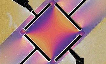
To achieve this feat, the scientists sliced very thin layers of CeIrIn5—only around a thousandth of a millimeter thick—that they joined to a sapphire substrate. When cooled, the material contracts significantly whereas the sapphire contracts very little. The resulting interaction puts stress on the material, as if it were being pulled in all directions, thus slightly distorting the atomic bonds in the slice. As the superconductivity in CeIrIn5 is unusually sensitive to the material’s exact atomic configuration, engineering a distortion pattern is all it takes to achieve a complex pattern of superconductivity. This new approach allows researchers to “draw” superconducting circuitry on a single crystal bar, a step that paves the way for new quantum technologies.
The image illustrates the temperature evolution of the spatially modulated superconducting state
This discovery represents a major step forward in controlling superconductivity in heavy fermion materials. But that’s not the end of the story. Following on from this project, a post-doc researcher has just begun exploring possible technological applications.
“We could, for example, change the regions of superconductivity by modifying the material’s distortion using a microactuator,” says Moll. “The ability to isolate and connect superconducting regions on a chip could also create a kind of switch for future quantum technologies, a little like the transistors used in today’s computing.”
Share on:


Suggested Items
Material Insight: The Dielectric Constant of PCB Materials
05/17/2024 | Dr. Preeya Kuray -- Column: Material InsightIn the world of PCB design, miniaturization can be achieved by using low dielectric constant (Dk) materials. Low Dk materials can allow for a reduction in thickness while maintaining a given trace width, leading to lower transmission loss and higher density circuitry.
IPC APEX EXPO: Some Thoughts About Growth
05/16/2024 | Dan Feinberg, I-Connect007After two and a half days of wandering the aisles at IPC APEX EXPO 2024, for the first time, I almost felt like I was exploring CES. There were so many booths and exhibits that I could describe, but I’d like to focus on the growth and huge value of this event, which has expanded well beyond just the growing and impressive exhibit show floor.
The Shaughnessy Report: Unlock Your High-speed Material Constraints
05/15/2024 | Andy Shaughnessy -- Column: The Shaughnessy ReportThe world of PCB materials used to be a fairly simple one. It was divided into two groups: the “traditional” laminates, often called FR-4, and the high-speed laminates developed especially for high-speed PCBs. These were two worlds that usually didn’t collide. But then traditional laminates started getting better, and high-speed designers and design engineers took notice and started to reconsider what FR-4 could be used for.
Breaking High-speed Material Constraints: Design007 Magazine — May 2024
05/14/2024 | I-Connect007 Editorial TeamDo you need specialty materials for your high-speed designs? Maybe not. Improvements in resins mean designers of high-speed boards can sometimes use traditional laminate systems instead of high-speed materials, saving time and money while streamlining the fab process. In the May 2024 issue of Design007 Magazine, our contributors explain how to avoid overconstraining your materials when working with high-speed boards.
Indium Experts to Present at Electronics in Harsh Environments SMTA Conference
05/13/2024 | Indium Corporationndium Corporation Technical Manager for Europe, Africa, and the Middle East, Karthik Vijay, will deliver a technical presentation and Indium Corporation Senior Technologist, Dr. Ronald Lasky, will deliver both a workshop and technical presentation at the Electronics in Harsh Environments SMTA Conference on May 14-16 in Copenhagen, Denmark.