


 It’s Only Common Sense: Nice Guys Really Can Finish First
 The Right Approach: I Hear the Train A Comin'
 Marcy's Musings: The Growing Industry
20% Efficient Solar Cell on EpiWafer
September 14, 2015 | Fraunhofer-GesellschaftEstimated reading time: 1 minute

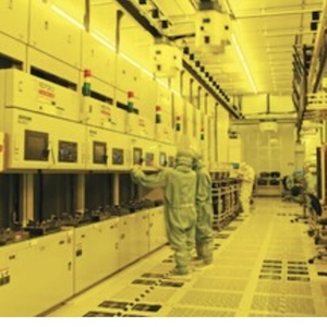
Recently NexWafe GmbH was spun out of the Fraunhofer Institute for Solar Energy Systems ISE, in order to bring the Institute’s kerfless EpiWafer technology to the market and rapid commercialization.
In the EpiWafer technology, a thick crystalline silicon layer is epitaxially deposited and subsequently detached after growth to produce a freestanding wafer of standard thickness.
Due to the radical changes in the manufacturing value chain, EpiWafers can be produced at an appreciably lower cost compared to the traditional wafer manufacturing process. The EpiWafer is a direct substitute for conventional n- or p-doped silicon mono-crystalline wafers.
Now, Fraunhofer ISE reports on substantial progress in the development of its EpiWafers, which are seen as a drop-in replacement for conventional Cz wafers. Fraunhofer ISE’s research team in co-operation with NexWafe has optimized all production steps for the EpiWafer.
Analysis of the new n-doped EpiWafers shows that mean minority carrier lifetimes are above 1000 µs, indicating the same quality as n-type Cz wafers. Solar cells processed on these EpiWafers yield 20% efficiency, independently confirmed at the Fraunhofer ISE CalLab. “I am elated about this fantastic result,” says Dr. Stefan Janz, Head of the Department of Silicon Materials.
“This success attests to our fast progress made in only a few months since focusing on EpiWafers.” The solar cells achieve a short-circuit current of 39.6 mA/cm2, a world-record value for epitaxially grown silicon solar cells. The new results will be presented during the coming European PVSEC in Hamburg.
Dr. Stefan Reber, CEO of NexWafe, is also very excited about the new results: “These values demonstrate that our EpiWafer technology is a game-changing technology. It accelerates the shift of the market towards high efficiency modules by providing high quality drop-in mono-crystalline EpiWafers at a very competitive price.”
Share on:


Suggested Items
IDTechEx Report on Quantum Technology: Nano-scale Physics for Massive Market Impact
04/30/2024 | PRNewswireThe quantum technology market leverages nano-scale physics to create revolutionary new devices for computing, sensing, and communications. Across the industry, quantum technology offers a paradigm shift in performance compared with incumbent solutions.
TSMC Certifies Ansys Multiphysics Platforms, Enabling Next-Gen AI and HPC Chips
04/30/2024 | PRNewswireAnsys announced the certification of its power integrity platforms for TSMC's N2 technology full production release. Both Ansys RedHawk-SC and Ansys Totem are certified for power integrity signoff on the N2 process, delivering significant speed and power advantages for high performance computing, mobile chips, and 3D-IC designs.
Koh Young Extends Invitation to the 2024 IEEE Electronic Components and Technology Conference
04/30/2024 | Koh YoungKoh Young, the industry leader in True3D measurement-based inspection solutions, invites you to join us at the at the 2024 IEEE Electronic Components and Technology Conference from May 28-31, 2024, in Denver, Colorado at the Gaylord Rockies Resort & Convention Center.
Samsung Electronics Begins Industry’s First Mass Production of 9th-Gen V-NAND
04/29/2024 | Samsung ElectronicsSamsung Electronics, the world leader in advanced memory technology, today announced that it has begun mass production for its one-terabit (Tb) triple-level cell (TLC) 9th-generation vertical NAND (V-NAND), solidifying its leadership in the NAND flash market.
TSMC Celebrates 30th North America Technology Symposium
04/29/2024 | TSMCTSMC unveiled its newest semiconductor process, advanced packaging, and 3D IC technologies for powering the next generation of AI innovations with silicon leadership at the Company’s 2024 North America Technology Symposium.