


 The Chemical Connection: Reducing Etch System Water Usage, Part 2
 It’s Only Common Sense: Nice Guys Really Can Finish First
 The Right Approach: I Hear the Train A Comin'
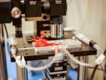
State-of-the-art atomic force microscopes (AFMs) are designed to capture images of structures as small as a fraction of a nanometer — a million times smaller than the width of a human hair. In recent years, AFMs have produced desktop-worthy close-ups of atom-sized structures, from single strands of DNA to individual hydrogen bonds between molecules.
But scanning these images is a meticulous, time-consuming process. AFMs therefore have been used mostly to image static samples, as they are too slow to capture active, changing environments.
Now engineers at MIT have designed an atomic force microscope that scans images 2,000 times faster than existing commercial models. With this new high-speed instrument, the team produced images of chemical processes taking place at the nanoscale, at a rate that is close to real-time video.
In one demonstration of the instrument’s capabilities, the researchers scanned a 70- by-70-micron sample of calcite as it was first immersed in deionized water and later exposed to sulfuric acid. The team observed the acid eating away at the calcite, expanding existing nanometer-sized pits in the material that quickly merged and led to a layer-by-layer removal of calcite along the material’s crystal pattern, over a period of several seconds.
Kamal Youcef-Toumi, a professor of mechanical engineering at MIT, says the instrument’s sensitivity and speed will enable scientists to watch atomic-sized processes play out as high-resolution “movies.”
“People can see, for example, condensation, nucleation, dissolution, or deposition of material, and how these happen in real-time — things that people have never seen before,” Youcef-Toumi says. “This is fantastic to see these details emerging. And it will open great opportunities to explore all of this world that is at the nanoscale.”
The group’s design and images, which are based on the PhD work of Iman Soltani Bozchalooi, now a postdoc in the Department of Mechanical Engineering, are published in the journal Ultramicroscopy.
Share on:


Suggested Items
TRI to Unveil New High-Throughput AOI and AXI at productronica 2023
09/15/2023 | TRITest Research, Inc. (TRI), the leading test and inspection systems provider for the electronics manufacturing industry, will join productronica 2023, which will be held at Messe München Center from November 14 – 17, 2023.
UK Space Agency Launches Consultation on Variable Liability Limits for Orbital Operations
09/15/2023 | UK Space AgencyThe proposals from the UK Space Agency follow a review into the UK’s approach to setting the amount of an operator’s liability in licences for orbital operations, a key commitment of the government’s National Space Strategy.
MediaTek Successfully Develops First Chip Using TSMC's 3nm Process, Set for Volume Production in 2024
09/14/2023 | MediaTekMediaTek and TSMC announced that MediaTek has successfully developed its first chip using TSMC's leading-edge 3nm technology, taping out MediaTek’s flagship Dimensity system-on-chip (SoC) with volume production expected next year.
MKS’ Atotech to Participate in IPCA Expo 2023
09/14/2023 | MKS’ AtotechMKS’ Atotech, a leading surface finishing brand of MKS Instruments, will participate in the upcoming IPCA Expo at Bangalore International Exhibition Centre (BIEC) and showcase its latest PCB manufacturing solutions from September 13 – 15.
Comtech Unveils New BRIDGE Solutions to Increase Access to Global Hybrid Connectivity
09/12/2023 | Business WireComtech launched its new blended, resilient, integrated, digital, global, end-to-end (BRIDGE) connectivity solutions. Comtech’s BRIDGE solutions provide portable, adaptable, full-service communications networks that can be established in a matter of hours and help “bridge the gap” for traditional satellite and terrestrial infrastructures.