


 The Right Approach: I Hear the Train A Comin'
 It’s Only Common Sense: OCCAM—the Time Is Now
 Marcy's Musings: The Growing Industry
Semiconductors with an Aligned Interface
November 13, 2017 | KAUSTEstimated reading time: 2 minutes
The electronic characteristics of an interface between two wide bandgap semiconductors are determined by researchers at KAUST, providing an insight that will help improve the efficiency of light-emitting and high-power electronic devices.
Semiconductors, such as silicon and gallium nitride, have electrical properties somewhere in between those of a conductor and an insulator. They only allow current to flow when electrons have enough energy to overcome a barrier known as bandgap. The bandgap—which may be direct or indirect, narrow or large—determines the properties of semiconductors and their consequent applications.
Materials with a large bandgap, for example, are useful in high-power electronics because they have larger breakdown voltage for energy-efficient transistors as compared with narrow bandgap materials, such as silicon. They can also produce light deep into the ultraviolet part of the spectrum, making them useful for disinfection and water purification.
These materials can be further tailored to a specific application by layering different semiconductors on top of each other to create a so-called heterostructure with the desired properties. But it is vital to understand how the bandgaps of two semiconductors align when semiconductors are brought together in this way.
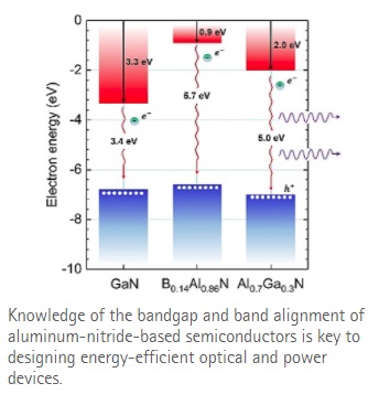
Haiding Sun and principle investigator Xiaohang Li from KAUST and coworkers from the Georgia Institute of Technology, USA, report that they experimentally measured the alignment of two emerging large bandgap materials: boron aluminum nitride and aluminum gallium nitride.
The 2014 Nobel Prize for physics was awarded in recognition of the development of gallium nitride light-emitting diodes. But, compared to gallium nitride, aluminum nitride has a much larger bandgap of 6.1 electronvolts. Its electronic properties can be tuned by replacing some of the aluminum atoms in the crystal with either boron or gallium.
The team created an interface between boron aluminum nitride with a boron to aluminum atom ratio of 14:86 and aluminum gallium nitride with a gallium nitride ratio of 30:70 on an aluminum-nitride-covered sapphire substrate.
They used high-resolution X-ray photoemission spectroscopy to measure the offset between the top and the bottom of the two material's bandgaps. They show that the bandgaps have a staggered alignment, with both the top and bottom edge of the bandgap of the Al0.7Ga0.3N lower than the respective edge in B0.14Al0.86N.
“Based on the experimental results, we can achieve a much higher amount of two-dimensional electron gas sheet carrier concentration in such junction,” says Sun. “The determination of the band alignment of B0.14Al0.86N/Al0.7Ga0.3N heterojunction provides valuable support in the design of optical and electronic devices based on such junctions.”
Share on:


Suggested Items
Real Time with... IPC APEX EXPO 2024: Sustainability in the Industry
04/26/2024 | Real Time with...IPC APEX EXPOGuest Editor Henry Crandall and Chris Nash of Indium Corporation discuss the company's 90th anniversary and its focus on sustainability. They focus on the benefits of sustainable materials, their compatibility, and value propositions. The conversation also highlights how Durafuse LT technology's role in reducing reflow temperatures is leading to significant cost and energy savings. Nash also touches on downstream sustainability efforts such as using recycled materials for packaging.
SMC Korea 2024 to Highlight Semiconductor Materials Trends and Innovations on Industry’s Path to $1 Trillion
04/24/2024 | SEMIWith Korea a major consumer of semiconductor materials and advanced materials a key driver of innovation on the industry’s path to $1 trillion, industry leaders and experts will gather at SMC (Strategic Materials Conference) Korea 2024 on May 29 at the Suwon Convention Center in Gyeonggi-do, South Korea to provide insights into the latest materials developments and trends. Registration is open.
Groundbreaking Ceremony Marks the Beginning of a New Era for Newccess Industrial; The Construction of the MINGXIN Building
04/12/2024 | Newccess IndustrialOn a clear and sunny day in March, the groundbreaking ceremony for the MINGXIN Building took place in Shenzhen, China. This moment marked the official commencement of construction for a project that will reshape the semiconductor materials industry.
The Need for a Holistic Global Sustainability Standard
04/10/2024 | Michael Ford, Aegis SoftwareNo one can deny that the resources of our fragile planet are finite. The environment seems like a third party, subject to constant degradation. We’re acutely aware of the effects of pollution on our climate, and despite our “throw-away” culture, recycling and recovery of materials has remained relatively expensive, even as we use more energy just to survive.
iNEMI Publishes Four Roadmap Topics
04/04/2024 | iNEMIThe International Electronics Manufacturing Initiative (iNEMI) announces the availability of the first roadmap topics in the new iNEMI Roadmap format. Printed circuit boards, sustainable electronics, smart manufacturing, and mmWave materials and test are now available online.