


 The Right Approach: I Hear the Train A Comin'
 It’s Only Common Sense: OCCAM—the Time Is Now
 Marcy's Musings: The Growing Industry
New Nanowires are Just a Few Atoms Thick
December 5, 2017 | MITEstimated reading time: 3 minutes
“Two-dimensional materials” — materials deposited in layers that are only a few atoms thick — are promising for both high-performance electronics and flexible, transparent electronics that could be layered onto physical surfaces to make computing ubiquitous.
The best-known 2-D material is graphene, which is a form of carbon, but recently researchers have been investigating other 2-D materials, such as molybdenum disulfide, which have their own, distinct advantages.
Producing useful electronics, however, requires integrating multiple 2-D materials in the same plane, which is a tough challenge. In 2015, researchers at King Abdullah University in Saudi Arabia developed a technique for depositing molybdenum disulfide (MoS2) next to tungsten diselenide (WSe2), with a very clean junction between the two materials. With a variation of the technique, researchers at Cornell University then found that they could induce long, straight wires of MoS2 — only a few atoms in diameter— to extend into the WSe2, while preserving the clean junction.
The researchers contacted Markus Buehler, the McAfee Professor of Engineering in MIT’s Department of Civil and Environmental Engineering, who specializes in atomic-level models of crack propagation, to see if his group could help explain this strange phenomenon.
In the latest issue of Nature Materials, the King Abdullah, Cornell, and MIT researchers team with colleagues at Academia Sinica, the Taiwanese national research academy, and Texas Tech University to describe both the material deposition method and the mechanism underlying the formation of the MoS2 nanowires, which the MIT researchers were able to model computationally.
“The manufacturing of new 2-D materials still remains a challenge,” Buehler says. “The discovery of mechanisms by which certain desired material structures can be created is key to moving these materials toward applications. In this process, the joint work of simulation and experiment is critical to make progress, especially using molecular-level models of materials that enable new design directions.”
Wired up
The ability to create long, thin MoS2 channels in WSe2 could have a number of applications, the researchers say.
“Based on [the materials’] electrical properties and optical properties, people are looking at using MoS2 and WSe2 for solar cells or for water splitting based on sunlight,” says Gang Seob Jung, an MIT graduate student in civil and environmental engineering and a coauthor on the new paper. “Most of the interesting stuff happens at the interface. When you have not just the one interface — if there are many nanowire interfaces — it could improve the efficiency of a solar cell, even if it’s quite random.”
But the theoretical explanation of the molecular mechanism underlying the nanowires’ formation also raises the hope that their formation could be controlled, to enable the assembly of atom-scale electronic components.
“Two-D materials, one of the most promising candidates for future electronics, ultimately need to beat silicon-based devices, which have achieved a few nanometers in size already,” says Yimo Han, a Cornell graduate student in chemistry and first author on the paper. “Two-D materials are the thinnest in the vertical direction but still span a quite large area in the lateral dimensions. We made the thinnest dislocation-free channels in 2-D materials, which is a big step toward subnanometer electronic devices out of 2-D materials.”
Propagating polygons
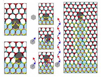
In a 2-D crystal, both MoS2 and WSe2 naturally arrange themselves into hexagons in which the constituent elements — molybdenum and sulfur or tungsten and selenium — alternate. Together, these hexagons produce a honeycomb pattern.
The Cornell researchers’ fabrication technique preserves this honeycomb pattern across the junction between materials, a rare feat and one that’s very useful for electronics applications. Their technique uses chemical vapor deposition, in which a substrate — in this case, sapphire — is exposed to gases carrying chemicals that react to produce the desired materials.
The natural sizes of the MoS2 and WSe2 hexagons are slightly different, however, so their integration puts a strain on both crystals, particularly near their junction. If a pair of WSe2 hexagons right at the MoS2 junction convert into a hexagon matched with a heptagon (a seven-sided polygon), it releases the strain.
This so-called 5|7 dislocation creates a site at which an MoS2 particle can attach itself. The resulting reaction inserts a molybdenum atom into the pentagon, producing a hexagon, and breaks the heptagon open. Sulfur atoms then attach to the heptagon to form another 5|7 dislocation. As this process repeats, the 5|7 dislocation moves deeper into WSe2 territory, with a nanowire extending behind it. The pattern in which the strain on the mismatched hexagons relaxes and recurs ensures that the dislocation progresses along a straight line.
The research was supported by the Office of Naval Research and the Department of Defense.
Share on:


Suggested Items
Book Excerpt: The Printed Circuit Assembler’s Guide to... Factory Analytics
04/24/2024 | I-Connect007 Editorial TeamIn our fast-changing, deeply competitive, and margin-tight industry, factory analytics can be the key to unlocking untapped improvements to guarantee a thriving business. On top of that, electronics manufacturers are facing a tremendous burden to do more with less. If you don't already have a copy of this book, what follows is an excerpt from the introduction chapter of 'The Printed Circuit Assembler’s Guide to... Factory Analytics: Unlocking Efficiency Through Data Insights' to whet your appetite.
Listen Up! The Intricacies of PCB Drilling Detailed in New Podcast Episode
04/25/2024 | I-Connect007In episode 5 of the podcast series, On the Line With: Designing for Reality, Nolan Johnson and Matt Stevenson continue down the manufacturing process, this time focusing on the post-lamination drilling process for PCBs. Matt and Nolan delve into the intricacies of the PCB drilling process, highlighting the importance of hole quality, drill parameters, and design optimization to ensure smooth manufacturing. The conversation covers topics such as drill bit sizes, aspect ratios, vias, challenges in drilling, and ways to enhance efficiency in the drilling department.
Elevating PCB Design Engineering With IPC Programs
04/24/2024 | Cory Blaylock, IPCIn a monumental stride for the electronics manufacturing industry, IPC has successfully championed the recognition of the PCB Design Engineer as an official occupation by the U.S. Department of Labor (DOL). This pivotal achievement not only underscores the critical role of PCB design engineers within the technology landscape, but also marks the beginning of a transformative journey toward nurturing a robust, skilled workforce ready to propel our industry into the future.
Winner of The Science Show Rakett 69 Receives Incap Scholarship
04/24/2024 | IncapThe winner of the Rakett 69 science show, Andri Türkson, who stood out as an electronics enthusiast, received a scholarship from Incap Estonia, along with an internship opportunity in Saaremaa.
Alternative Manufacturing Inc. Awarded QML Requalification to IPC J-STD-001 and IPC-A-610
04/24/2024 | IPCIPC's Validation Services Program has awarded an IPC J-STD-001 and IPC-A-610 Qualified Manufacturers Listing (QML) requalification to Alternative Manufacturing Inc (AMI).