


 The Right Approach: I Hear the Train A Comin'
 It’s Only Common Sense: OCCAM—the Time Is Now
 Marcy's Musings: The Growing Industry
Engineers Develop Efficient Semiconductor Material for Thermal Management
July 20, 2018 | UCLAEstimated reading time: 2 minutes
Working to address “hotspots” in computer chips that degrade their performance, UCLA engineers have developed a new semiconductor material, defect-free boron arsenide, that is more effective at drawing and dissipating waste heat than any other known semiconductor or metal materials.
This could potentially revolutionize thermal management designs for computer processors and other electronics, or for light-based devices like LEDs.
Computer processors have continued to shrink down to nanometer sizes where today there can be billions of transistors are on a single chip. This phenomenon is described under Moore’s Law, which predicts that the number of transistors on a chip will double about every two years. Each smaller generation of chips helps make computers faster, more powerful and able to do more work. But doing more work also means they’re generating more heat.
Managing heat in electronics has increasingly become one of the biggest challenges in optimizing performance. High heat is an issue for two reasons. First, as transistors shrink in size, more heat is generated within the same footprint. This high heat slows down processor speeds, in particular at “hotspots” on chips where heat concentrates and temperatures soar. Second, a lot of energy is used to keep those processors cool. If CPUs did not get as hot in the first place, then they could work faster and much less energy would be needed to keep them cool.
Image caption: Illustration showing a schematic of a computer chip with a hotspot (bottom); an electron microscope image of defect-free boron arsenide (middle); and an image showing electron diffraction patterns in boron arsenide. Image credit: Hu Research Lab/UCLA Samueli
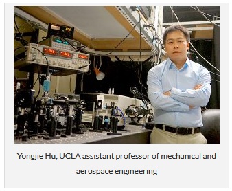
The UCLA study was the culmination of several years of research by Hu and his students that included designing and making the materials, predictive modeling, and precision measurements of temperatures.
The defect-free boron arsenide, which was made for first time by the UCLA team, has a record-high thermal conductivity, more than three-times faster at conducting heat than currently used materials, such as silicon carbide and copper, so that heat that would otherwise concentrate in hotspots is quickly flushed away.
“This material could help greatly improve performance and reduce energy demand in all kinds of electronics, from small devices to the most advanced computer data center equipment,” Hu said. “It has excellent potential to be integrated into current manufacturing processes because of its semiconductor properties and the demonstrated capability to scale-up this technology. It could replace current state-of-the-art semiconductor materials for computers and revolutionize the electronics industry.”
In addition to the impact for electronic and photonics devices, the study also revealed new fundamental insights into the physics of how heat flows through a material.
“This success exemplifies the power of combining experiments and theory in new materials discovery, and I believe this approach will continue to push the scientific frontiers in many areas, including energy, electronics, and photonics applications,” Hu said.
The research was funded by the National Science Foundation, the Air Force Office of Scientific Research, the American Chemical Society’s Petroleum Research Fund, UCLA’s Sustainable LA Grand Challenge, and the Anthony and Jeanne Pritzker Family Foundation.
Share on:


Suggested Items
Warm Windows and Streamlined Skin Patches – IDTechEx Explores Flexible and Printed Electronics
04/26/2024 | IDTechExFlexible and printed electronics can be integrated into cars and homes to create modern aesthetics that are beneficial and easy to use. From luminous car controls to food labels that communicate the quality of food, the uses of this technology are endless and can upgrade many areas of everyday life.
Book Excerpt: The Printed Circuit Assembler’s Guide to... Factory Analytics
04/24/2024 | I-Connect007 Editorial TeamIn our fast-changing, deeply competitive, and margin-tight industry, factory analytics can be the key to unlocking untapped improvements to guarantee a thriving business. On top of that, electronics manufacturers are facing a tremendous burden to do more with less. If you don't already have a copy of this book, what follows is an excerpt from the introduction chapter of 'The Printed Circuit Assembler’s Guide to... Factory Analytics: Unlocking Efficiency Through Data Insights' to whet your appetite.
Listen Up! The Intricacies of PCB Drilling Detailed in New Podcast Episode
04/25/2024 | I-Connect007In episode 5 of the podcast series, On the Line With: Designing for Reality, Nolan Johnson and Matt Stevenson continue down the manufacturing process, this time focusing on the post-lamination drilling process for PCBs. Matt and Nolan delve into the intricacies of the PCB drilling process, highlighting the importance of hole quality, drill parameters, and design optimization to ensure smooth manufacturing. The conversation covers topics such as drill bit sizes, aspect ratios, vias, challenges in drilling, and ways to enhance efficiency in the drilling department.
Elevating PCB Design Engineering With IPC Programs
04/24/2024 | Cory Blaylock, IPCIn a monumental stride for the electronics manufacturing industry, IPC has successfully championed the recognition of the PCB Design Engineer as an official occupation by the U.S. Department of Labor (DOL). This pivotal achievement not only underscores the critical role of PCB design engineers within the technology landscape, but also marks the beginning of a transformative journey toward nurturing a robust, skilled workforce ready to propel our industry into the future.
Winner of The Science Show Rakett 69 Receives Incap Scholarship
04/24/2024 | IncapThe winner of the Rakett 69 science show, Andri Türkson, who stood out as an electronics enthusiast, received a scholarship from Incap Estonia, along with an internship opportunity in Saaremaa.