


 The Right Approach: I Hear the Train A Comin'
 It’s Only Common Sense: OCCAM—the Time Is Now
 Marcy's Musings: The Growing Industry
Probing Individual Edge States With Unprecedented Precision
September 12, 2018 | University of BaselEstimated reading time: 2 minutes
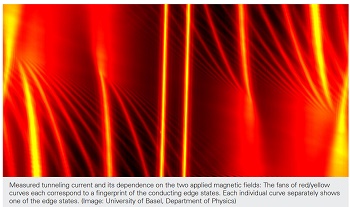
A new technique makes it possible to obtain an individual fingerprint of the current-carrying edge states occurring in novel materials such as topological insulators or 2D materials.
While insulators do not conduct electrical currents, some special materials exhibit peculiar electrical properties: though not conducting through their bulk, their surfaces and edges may support electrical currents due to quantum mechanical effects, and do so even without causing losses.
Such so-called topological insulators have attracted great interest in recent years due to their remarkable properties. In particular, their robust edge states are very promising since they could lead to great technological advances.
Currents Flowing Only Along the Edges
Similar effects as the edge states of such topological insulators also appear when a two-dimensional metal is exposed to a strong magnetic field at low temperatures. When the so-called quantum Hall effect is realized, current is thought to flow only at the edges, where several conducting channels are formed.
Probing Individual Edge States
Until now, it was not possible to address the numerous current carrying states individually or to determine their positions separately. The new technique now makes it possible to obtain an exact fingerprint of the current carrying edge states with nanometer resolution.
This is reported by researchers of the Department of Physics and the Swiss Nanoscience Institute of the University of Basel in collaboration with colleagues of the University of California, Los Angeles, as well as of Harvard and Princeton University, USA.
In order to measure the fingerprint of the conducting edge states, the physicists lead by Prof. Dominik Zumbühl have further developed a technique based on tunneling spectroscopy.
They have used a gallium arsenide nanowire located at the sample edge which runs in parallel to the edge states under investigation. In this configuration, electrons may jump (tunnel) back and forth between a specific edge state and the nanowire as long as the energies in both systems coincide. Using an additional magnetic field, the scientists control the momentum of tunneling electrons and can address individual edge states. From the measured tunneling currents, the position and evolution of each edge state may be obtained with nanometer precision.
Tracking the Evolution
This new technique is very versatile and can also be used to study dynamically evolving systems. Upon increasing the magnetic field, the number of edge states is reduced, and their distribution is modified. For the first time, the scientists were able to watch the full edge state evolution starting from their formation at very low magnetic fields.
With increasing magnetic field, the edge states are first compressed towards the sample boundary until eventually, they move towards the inside of the sample and then disappear completely. Analytical and numerical models developed by the research team agree very well with the experimental data.
“This new technique is not only very useful to study the quantum Hall edge states,” Dominik Zumbühl comments the results of the international collaboration. “It might also be employed to investigate new exotic materials such as topological insulators, graphene or other 2D materials.”
Share on:


Suggested Items
SMC Korea 2024 to Highlight Semiconductor Materials Trends and Innovations on Industry’s Path to $1 Trillion
04/24/2024 | SEMIWith Korea a major consumer of semiconductor materials and advanced materials a key driver of innovation on the industry’s path to $1 trillion, industry leaders and experts will gather at SMC (Strategic Materials Conference) Korea 2024 on May 29 at the Suwon Convention Center in Gyeonggi-do, South Korea to provide insights into the latest materials developments and trends. Registration is open.
Groundbreaking Ceremony Marks the Beginning of a New Era for Newccess Industrial; The Construction of the MINGXIN Building
04/12/2024 | Newccess IndustrialOn a clear and sunny day in March, the groundbreaking ceremony for the MINGXIN Building took place in Shenzhen, China. This moment marked the official commencement of construction for a project that will reshape the semiconductor materials industry.
The Need for a Holistic Global Sustainability Standard
04/10/2024 | Michael Ford, Aegis SoftwareNo one can deny that the resources of our fragile planet are finite. The environment seems like a third party, subject to constant degradation. We’re acutely aware of the effects of pollution on our climate, and despite our “throw-away” culture, recycling and recovery of materials has remained relatively expensive, even as we use more energy just to survive.
iNEMI Publishes Four Roadmap Topics
04/04/2024 | iNEMIThe International Electronics Manufacturing Initiative (iNEMI) announces the availability of the first roadmap topics in the new iNEMI Roadmap format. Printed circuit boards, sustainable electronics, smart manufacturing, and mmWave materials and test are now available online.
Insulectro’s 'Storekeepers' Extend Their Welcome to Technology Village at IPC APEX EXPO
04/03/2024 | InsulectroInsulectro, the largest distributor of materials for use in the manufacture of PCBs and printed electronics, welcomes attendees to its TECHNOLOGY VILLAGE during this year’s IPC APEX EXPO at the Anaheim Convention Center, April 9-11, 2024.