


 The Right Approach: I Hear the Train A Comin'
 It’s Only Common Sense: OCCAM—the Time Is Now
 Marcy's Musings: The Growing Industry
Goodbye, Silicon?
October 17, 2018 | MAX-PLANCK-GESELLSCHAFTEstimated reading time: 3 minutes
Scientists at the Max Planck Institute for Polymer Research (MPI-P) in Mainz (Germany) together with scientists from Dresden, Leipzig, Sofia (Bulgaria) and Madrid (Spain) have now developed and characterized a novel, metal-organic material which displays electrical properties mimicking those of highly crystalline silicon. The material which can easily be fabricated at room temperature could serve as a replacement for expensive conventional inorganic materials used in optoelectronics.
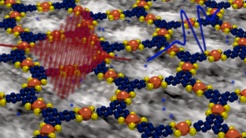
Image Caption: A metal-organic framework could serve as a replacement for the semiconductor silicon in the future. Image: MPI-P, License CC-BY-SA
Silicon, a so called semiconductor, is currently widely employed for the development of components such as solar cells, LEDs or computer chips. High purity silicon, a highly ordered material which is expensive to produce, is required to develop such applications. This is due to the fact that the electrical properties of a semiconductor (as silicon) are strongly affected by disorder. The scientists around group leader Enrique Cánovas (MPI-P, Department of Prof. Dr. Mischa Bonn) have now developed a novel low cost metal-organic framework (MOF), which has similar electrical properties.
The MOF, produced by Xinliang Feng´s group in Dresden, is a highly crystalline solid made of iron ions linked by organic molecules, hence the name metal-organic framework. In contrast to silicon, the material can be made at room temperature, and the sample chemistry, morphology and electronic properties are easily customizable during the manufacturing process.
MOFs produced in the past showed no or very little electrical conductivity, this prevented MOFs to be employed in optoelectronic applications, where an “easy” displacement of electrons under an applied electrical field is required. With the novel MOF, the researchers from Mainz have now demonstrated - for an organic-based material - a behavior of the conductivity similar to silicon, a so-called "Drude behavior" (named after the physicist Paul Drude). A Drude behavior implies that electrons within the material are almost free to move under the application of an external electric field, i.e. if a voltage is applied. This behavior, a common observable for highly ordered inorganic crystals like silicon, has been hardly seen in organic based materials; organic based materials are generally disordered in nature, unlike MOFs.
To characterize the unique properties for the developed MOF, the scientists at MPI-P employed ultrafast terahertz spectroscopy, a tool that allows measuring the conductivity of the material without requiring physical – perturbative - contacts. Using this tool, energy is transferred to the electrons in the semicondcuting material due to the absorption of light (mediated by an ultrafast laser pump pulse in the visible region). A second laser pulse - a so-called terahertz probe, which oscillates about a factor of 1000 slower than visible light – allows to interrogate the conductivity for the photo-generated electrons. This results in a frequency dependent conductivity signal from which the scientists were able to model by “Drude” the nature of the transport of the electrons in the MOF. “From this response, we obtained record mobilities of the electrons in such materials which exceed the mobilities measured in insulating MOFs by a factor of 10000”, says Dr. Enrique Canovas of the MPI-P. This means that electrons can easily drift under an electric field over long distances in MOFs, an aspect that was independently verified in ~1000 micron length devices. Thus, the new material paves the way for the use of MOFs in optoelectronics.
In the future, the researchers will work on the ability to directly set and predict the electronic properties via tuning the composition of their produced metal-organic framework. Their research results have now been published in the renowned journal Nature Materials.
About Enrique Cánovas
Enrique Cánovas graduated on Applied Physics at the Universidad Autónoma de Madrid and holds a PhD, also in Physics, at the Polytechnic University of Madrid where he focused on the exploitation of quantum dots for the development of high-efficiency solar cells. After a 2 years postdoc at FOM Institute AMOLF (The Netherlands), in 2012, he was appointed group leader in the Department of Molecular Spectroscopy (Prof. Mischa Bonn) at the Max Planck Institute for Polymer Research. Since April 2018, he is Research Professor (tenure track) at IMDEA Nanoscience in Madrid (Spain). His research interests cover all aspects of nanotechnology, solar energy conversion and charge carrier dynamics.
Share on:


Suggested Items
Water Management in a Large Printed Circuit Board Manufacturer
04/15/2024 | Charles Nehrig, TTM TechnologiesTTM’s environmental management is grounded in its Environmental Statement and Environmental Policy, which promote measures that make for a more responsible environmental management process. Our management system helps TTM work toward minimizing its environmental footprint and increasing the sustainability of its operations. TTM monitors its environmental performance just as it monitors its operational performance, and provides the resources required to adhere to the Company’s environmental responsibilities.
Happy’s Tech Talk #27: Integrated Mesh Power System (IMPS) for PCBs
04/08/2024 | Happy Holden -- Column: Happy’s Tech TalkA significant decrease in HDI substrate production cost can be achieved by reducing the number of substrate layers from conventional through-hole multilayers and microvia multilayers of eight, 10, 12, and more to only two layers. Besides reducing direct processing steps, the yield will increase as defect-producing operations are eliminated. The integrated mesh power system (IMPS) was invented in the latter years of MCM-D use for thin-film fabrication. Those geometries fit today into our use of ultra HDI.
Trouble in Your Tank: Supporting IC Substrates and Advanced Packaging, Part 5
03/19/2024 | Michael Carano -- Column: Trouble in Your TankDirect metallization systems based on conductive graphite or carbon dispersion are quickly gaining acceptance worldwide. Indeed, the environmental and productivity gains one can achieve with these processes are outstanding. In today’s highly competitive and litigious environment, direct metallization reduces costs associated with compliance, waste treatment, and legal issues related to chemical exposure. What makes these processes leaders in the direct metallization space?
Indium Corporation Experts to Present at SEMI THERM
03/07/2024 | Indium CorporationIndium Corporation Global Account Manager and Senior Thermal Technologist Tim Jensen and Product Development Specialist for Thermal Interface Materials Miloš Lazić will present on thermal interface material (TIM) technology at SEMI-THERM, taking place March 25–28 in San Jose, California, U.S.
Indium Corporation to Showcase Proven EV Products and High-Reliability Alloys at Productronica China
02/28/2024 | Indium CorporationAs a materials pioneer and trusted partner in electric vehicle (EV) and e-Mobility manufacturing, Indium Corporation is proud to showcase its high-reliability alloys and soldering solutions at Productronica China, March 20-22, in Shanghai.