


 The Right Approach: I Hear the Train A Comin'
 It’s Only Common Sense: OCCAM—the Time Is Now
 Marcy's Musings: The Growing Industry
Semiconductor Scientists Discover Effect That Was Thought Impossible
April 23, 2019 | MIPTEstimated reading time: 3 minutes
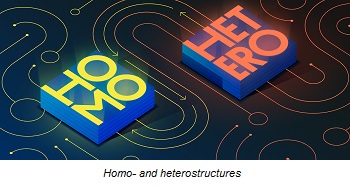
A physical effect known as superinjection underlies modern light-emitting diodes (LEDs) and lasers. For decades this effect was believed to occur only in semiconductor heterostructures — that is, structures composed of two or more semiconductor materials. Researchers from the Moscow Institute of Physics and Technology have found superinjection to be possible in homostructures, which are made of a single material. This opens up entirely new prospects for the development of light sources.
Semiconductor light sources, such as lasers and LEDs, are at the core of modern technology. They enable laser printers and high-speed internet. But a mere 60 years ago, no one would imagine semiconductors being used as materials for bright light sources. The problem was that to generate light, such devices require electrons and holes — the free charge carriers in any semiconductor — to recombine. The higher the concentration of electrons and holes, the more often they recombine, making the light source brighter. However, for a long time, no semiconductor device could be manufactured to provide a sufficiently high concentration of both electrons and holes.
The solution was found in the 1960s by Zhores Alferov and Herbert Kroemer. They proposed to use heterostructures, or “sandwich” structures, consisting of two or more complementary semiconductors instead of just one. If one places a semiconductor between two semiconductors with wider bandgaps and applies a forward bias voltage, the concentration of electrons and holes in the middle layer can reach values that are orders of magnitude higher than those in the outer layers. This effect, known as superinjection, underlies modern semiconductor lasers and LEDs. Its discovery earned Alferov and Kroemer the Nobel Prize in physics in 2000.
However, two arbitrary semiconductors cannot make a viable heterostructure. The semiconductors need to have the same period of the crystal lattice. Otherwise, the number of defects at the interface between the two materials will be too high, and no light will be generated. In a way, this would be similar to trying to screw a nut on a bolt whose thread pitch does not match that of the nut. Since homostructures are composed of just one material, one part of the device is a natural extension of the other. Although homostructures are easier to fabricate, it was believed that homostructures could not support superinjection and therefore are not a viable basis for practical light sources.
Igor Khramtsov and Dmitry Fedyanin from the Moscow Institute of Physics and Technology made a discovery that drastically changes the perspective on how light-emitting devices can be designed. The physicists found that it is possible to achieve superinjection with just one material. What is more, most of the known semiconductors can be used.
“In the case of silicon and germanium, superinjection requires cryogenic temperatures, and this casts doubt on the utility of the effect. But in diamond or gallium nitride, strong superinjection can occur even at room temperature,” Dr. Fedyanin said. This means that the effect can be used to create mass market devices. According to the new paper, superinjection can produce electron concentrations in a diamond diode that are 10,000 times higher than those previously believed to be ultimately possible. As a result, diamond can serve as the basis for ultraviolet LEDs thousands of times brighter than what the most optimistic theoretical calculations predicted. “Surprisingly, the effect of superinjection in diamond is 50 to 100 times stronger than that used in most mass market semiconductor LEDs and lasers based on heterostructures,” Khramtsov pointed out.
The physicists emphasized that superinjection should be possible in a wide range of semiconductors, from conventional wide-bandgap semiconductors to novel two-dimensional materials. This opens up new prospects for designing highly efficient blue, violet, ultraviolet, and white LEDs, as well as light sources for optical wireless communication (Li-Fi), new types of lasers, transmitters for the quantum internet, and optical devices for early disease diagnostics.
Share on:


Suggested Items
Real Time with... IPC APEX EXPO 2024: Sustainability in the Industry
04/26/2024 | Real Time with...IPC APEX EXPOGuest Editor Henry Crandall and Chris Nash of Indium Corporation discuss the company's 90th anniversary and its focus on sustainability. They focus on the benefits of sustainable materials, their compatibility, and value propositions. The conversation also highlights how Durafuse LT technology's role in reducing reflow temperatures is leading to significant cost and energy savings. Nash also touches on downstream sustainability efforts such as using recycled materials for packaging.
SMC Korea 2024 to Highlight Semiconductor Materials Trends and Innovations on Industry’s Path to $1 Trillion
04/24/2024 | SEMIWith Korea a major consumer of semiconductor materials and advanced materials a key driver of innovation on the industry’s path to $1 trillion, industry leaders and experts will gather at SMC (Strategic Materials Conference) Korea 2024 on May 29 at the Suwon Convention Center in Gyeonggi-do, South Korea to provide insights into the latest materials developments and trends. Registration is open.
Groundbreaking Ceremony Marks the Beginning of a New Era for Newccess Industrial; The Construction of the MINGXIN Building
04/12/2024 | Newccess IndustrialOn a clear and sunny day in March, the groundbreaking ceremony for the MINGXIN Building took place in Shenzhen, China. This moment marked the official commencement of construction for a project that will reshape the semiconductor materials industry.
The Need for a Holistic Global Sustainability Standard
04/10/2024 | Michael Ford, Aegis SoftwareNo one can deny that the resources of our fragile planet are finite. The environment seems like a third party, subject to constant degradation. We’re acutely aware of the effects of pollution on our climate, and despite our “throw-away” culture, recycling and recovery of materials has remained relatively expensive, even as we use more energy just to survive.
iNEMI Publishes Four Roadmap Topics
04/04/2024 | iNEMIThe International Electronics Manufacturing Initiative (iNEMI) announces the availability of the first roadmap topics in the new iNEMI Roadmap format. Printed circuit boards, sustainable electronics, smart manufacturing, and mmWave materials and test are now available online.